Unlock instant, AI-driven research and patent intelligence for your innovation.

Liquid crystal display device, array substrate thereof and manufacturing method of array substrate

A technology of liquid crystal display devices and array substrates, which is applied in the fields of nonlinear optics, instruments, optics, etc., can solve problems such as difficulty in realizing thin design and limitations, and achieve the effects of reducing energy consumption, reducing thickness, and saving costs

Inactive Publication Date: 2016-01-27
TCL CHINA STAR OPTOELECTRONICS TECH CO LTD
View PDF5 Cites 8 Cited by
  • Summary
  • Abstract
  • Description
  • Claims
  • Application Information

AI Technical Summary

Problems solved by technology

However, the direct-lit backlight module is limited by the secondary optical lens, which makes it difficult to achieve a thin design; while the edge-lit backlight module is limited by the light guide plate, it is also difficult to achieve a thin design

Method used


Image

  • Liquid crystal display device, array substrate thereof and manufacturing method of array substrate
  • Liquid crystal display device, array substrate thereof and manufacturing method of array substrate
  • Liquid crystal display device, array substrate thereof and manufacturing method of array substrate

Examples


Embodiment Construction

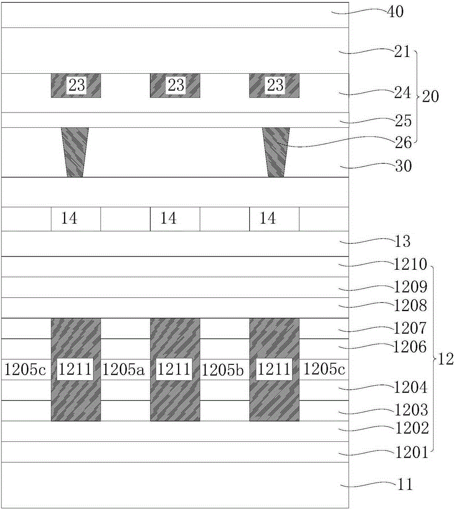
[0021] Hereinafter, embodiments of the present invention will be described in detail with reference to the accompanying drawings. This invention may, however, be embodied in many different forms and should not be construed as limited to the specific embodiments set forth herein. Rather, the embodiments are provided to explain the principles of the invention and its practical application, thereby enabling others skilled in the art to understand the invention for various embodiments and with various modifications as are suited to particular intended uses.

[0022] In the drawings, the thicknesses of layers and regions are exaggerated for device clarity. Like reference numerals refer to like elements throughout the drawings.

[0023] It will be understood that, although the terms "first", "second", etc. may be used herein to describe various elements, these elements should not be limited by these terms. These terms are only used to distinguish one element from another.

[0024...


PUM

PropertyMeasurementUnit
thicknessaaaaaaaaaa
thicknessaaaaaaaaaa

Abstract

The invention discloses a liquid crystal display device. The liquid crystal display device comprises a first substrate (11), a three-color light organic light emitting diode (12) arranged on the first substrate (11), a plurality of switch elements (14) arranged on the three-color light organic light emitting diode (12) in an array shape, a liquid crystal layer (30) arranged on the switch elements (14), and an upper substrate (20) arranged on the liquid crystal layer (30). The invention further discloses an array substrate and a manufacturing method thereof. Due to the fact that the three-color light organic light emitting diode is integrated and manufactured on the array substrate, the thickness of the liquid crystal display device can be substantially reduced. Beside, due to the fact that the three-color light organic light emitting diode is used for replacing LEDs in the prior art to serve as a backlight light-emitting device and the energy consumption of the three-color light organic light emitting diode is far smaller than that of the LEDs, the energy consumption of the liquid crystal display device can be reduced, and cost can be saved.

Description

technical field [0001] The invention belongs to the technical field of liquid crystal display, and in particular relates to a liquid crystal display device, an array substrate thereof, and a manufacturing method of the array substrate. Background technique [0002] With the evolution of optoelectronics and semiconductor technology, it has also led to the vigorous development of Flat Panel Displays. Among many flat panel displays, Liquid Crystal Displays (LCD for short) have high space utilization efficiency, low power consumption, no radiation and Low electromagnetic interference and many other superior features have become the mainstream of the market. [0003] In the existing liquid crystal display, it mainly includes a liquid crystal panel and a backlight module arranged oppositely. Since the liquid crystal panel itself does not emit light, a backlight module is required to provide it with a display light source. In the backlight module, the mainstream light-emitting de...

Claims


Application Information

Patent Timeline
Patent Type & Authority Applications(China)
IPC IPC(8): G02F1/13357G02F1/1333
CPCG02F1/133603G02F1/133621
Inventor 徐向阳
Owner TCL CHINA STAR OPTOELECTRONICS TECH CO LTD