Semiconductor device

A semiconductor, integrated technology, applied in the direction of semiconductor devices, semiconductor/solid-state device components, electric solid-state devices, etc., can solve the problems of water and other foreign objects entering, through-hole deformation, etc., to achieve the effect of reducing the size of the device

Active Publication Date: 2016-01-27
LAPIS SEMICON CO LTD
View PDF5 Cites 4 Cited by
  • Summary
  • Abstract
  • Description
  • Claims
  • Application Information

AI Technical Summary

Problems solved by technology

Therefore, when it is assumed that a through hole directly connected to the internal circuit is provided directly under the pad, not only the possibility of deforming the through hole due to the above-mentioned physical force, but also foreign matter such as water entering the possibility of

Method used


Image

  • Semiconductor device
  • Semiconductor device
  • Semiconductor device

Examples


Embodiment Construction

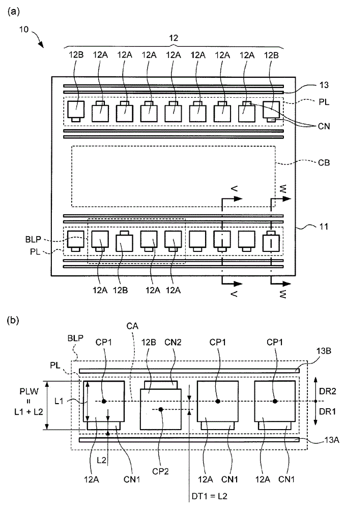
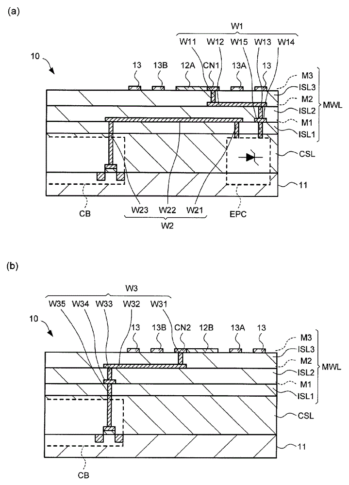
[0023] figure 1 (a) is a diagram schematically showing the upper surface of the semiconductor device 10 of the first embodiment. The semiconductor device 10 has a structure in which a circuit block CB is formed in a semiconductor substrate (hereinafter, simply referred to as a substrate) 11 . The circuit block CB is formed at the center of the substrate 11 in plan view when viewed from a direction perpendicular to the substrate 11 . In this embodiment, a case where the substrate 11 and the circuit block CB have a rectangular shape in plan view will be described.

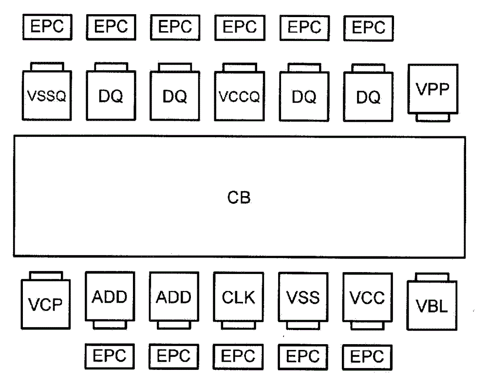
[0024] The semiconductor device 10 has a pad group 12 composed of a plurality of pads. Each of the plurality of pads is formed with a connection portion CN extending from each of the pads and connected to the wiring to the circuit block CB. Each of the connection parts CN constitutes an extraction part of a pad. In addition, a plurality of pads are arranged in one row, and a pad row PL is formed as a whole includ...


PUM


Abstract

The present invention relates to semiconductor devices. The present invention provides a semiconductor device can optimize the layout of welding pads and an extraction part, and cut down the device size. The semiconductor device comprises: a pad group including a plurality of pads provided on a semiconductor substrate and arranged in a row to form a pad row as a whole. The pad group includes: at least one first pad provided with a first via-connection part electrically connected therewith and extended in a first direction perpendicular to a row direction of the pad row; and at least one second pad provided with a second via-connection part electrically connected therewith and extended in a second direction opposite to the first direction. The at least one second pad is formed at a position moved in the first direction from the row direction of the pad row passing through a center of the at least one first pad.

Description

technical field [0001] The present invention relates to a semiconductor device, and more particularly, to a pad layout of a semiconductor device. Background technique [0002] Semiconductor devices such as semiconductor integrated circuits have more complicated circuit blocks along with their higher functionality and larger size. In addition, more pads are provided as connection interfaces with the outside in the semiconductor device. Therefore, in order to reduce the size of a semiconductor device, it is necessary not only to miniaturize the circuit block but also to design the device including pad layout and wiring from the pad to the circuit block. [0003] For example, Patent Document 1 discloses a semiconductor integrated circuit including an internal cell region formed in the center of a substrate, a plurality of input / output cells formed around the internal cell region and arranged in multiple columns, and a The plurality of pads on the peripheral portion of the sub...

Claims


Application Information

Patent Timeline
Patent Type & Authority Applications(China)
IPC IPC(8): H01L23/482
CPCH01L24/06H01L27/0251H01L2224/04042H01L2224/05548H01L2224/05553H01L2224/06155H01L2224/09515H01L2924/00014H01L2924/00012H01L2224/45099H01L2224/45015H01L2924/207H01L24/49H01L2224/0557H01L2224/06515H01L2224/0801
Inventor 那须信敬
Owner LAPIS SEMICON CO LTD
Why Eureka
Try Eureka