Camera module set

A camera module and image sensor technology, applied in radiation control devices and other directions, can solve the problems of difficult manufacturing reliability, high clean room level, and long cycle.

Pending Publication Date: 2016-01-27
GALAXYCORE SHANGHAI
View PDF4 Cites 11 Cited by
  • Summary
  • Abstract
  • Description
  • Claims
  • Application Information

AI Technical Summary

Problems solved by technology

However, CSP packaging has the following obvious problems: 1 affects product performance: the absorption, refraction, reflection and scattering of light by thick support glass have a great impact on the performance of image sensors, especially small pixel size products; 2 reliability issues : The thermal expansion coefficient difference between the components in the package structure and the sealing gas in the cavity have reliability problems in the subsequent SMT process or changes in the product use environment; 3 Large investment scale, large environmental pollution control requirements, and long production cycle , the unit chip cost is high, especially for high-pixel and large-size image sensor products
On the one hand, the stability of the camera module mainly depends on the peripheral bonding structure 41 formed by the mounting frame 4 and the circuit substrate 2, which is easily affected by external factors such as temperature and pressure, and the stability of the module needs to be strengthened; on the other hand, the direct light incident on the pads 12 and / or bonding wires 6 on the periphery of the photosensitive region 11 of the image sensor chip 1 (such as figure 1 As shown by the middle arrow), a large amount of stray light (flare) is generated, and high-end pixel products have higher requirements for stray light, and products with severe stray light cannot meet their quality requirements
In addition, COB packaging has the following obvious problems: 1. Dust control is very difficult, requiring ultra-high clean room levels, and high manufacturing maintenance costs; 2. Product design customization, long cycle, and insufficient flexibility; 3. Difficult to scale chemical production
However, the FC package has the following obvious problems: 1. The package has high requirements on the PCB substrate, and has a similar thermal expansion coefficient to Si, and the cost is very high; 2. Manufacturing reliability is very difficult, and the connection between all the bumps and pads of the thermosonic is consistent. Very high performance requirements, hard connection between bumps and pads, poor ductility; 3 Difficult to control dust, high requirements on process environment, and high cost

Method used


Image

  • Camera module set
  • Camera module set
  • Camera module set

Examples


Embodiment 1

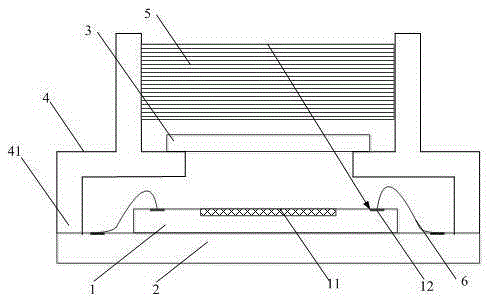
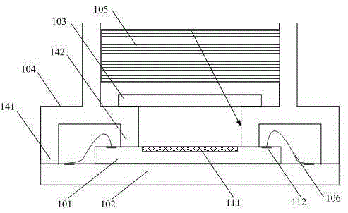
[0026] figure 2 It is a schematic structural diagram of a camera module according to Embodiment 1 of the present invention. The camera module includes an image sensor chip 101, a mounting frame 104, and a circuit substrate 102, and an inner layer support structure 142 is added on the peripheral bonding structure 141 between the installation frame 104 and the circuit substrate 102, and the inner layer support structure 142 Contacting the periphery of the photosensitive area 111 of the image sensor chip 101 makes the camera module more robust.

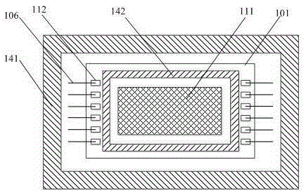
[0027] Wherein, the inner support structure 142 and the image sensor chip 101 can form a closed structure or an open structure. image 3 It is a top view of the closed structure of the camera module according to Embodiment 1 of the present invention; Figure 4 , Figure 5 It is a top view of the open structure of the camera module according to Embodiment 1 of the present invention.

[0028] Such as image 3 As shown, usually the im...

Embodiment 2

[0032] Figure 6 It is a schematic structural diagram of a camera module according to Embodiment 2 of the present invention. The camera module includes an image sensor chip 201, a mounting frame 204, and a circuit substrate 202, and an inner support structure 242 is added on the peripheral bonding structure 241 of the mounting frame 204 and the circuit substrate 202, and the inner support structure 242 Contacting the periphery of the photosensitive area 211 of the image sensor chip 201 makes the camera module more robust.

[0033] Different from Embodiment 1, the inner support structure 242 in this embodiment cannot be arranged between the photosensitive region 211 and the pad 212, but can only be arranged in the non-pad area around the photosensitive region 211, such as Figure 7 As shown in the horizontal extension of the inner support structure 242, the inner support structure 242 and the photosensitive surface of the image sensor chip 201 form a stepped inner cavity, which ...


PUM


Abstract

The invention provides a camera module set. The camera module set includes an image sensor chip, a mounting frame and a circuit board substrate; an inner layer supporting structure is additionally arranged on a peripheral bonding structure formed by the mounting frame and the circuit board substrate; the inner layer supporting structure contacts with the periphery of a photosensitive region of the image sensor chip; and therefore, the camera module set can be firmer. The inner layer supporting structure can prevent light from directly entering pads and/or bond lines, or the inner layer supporting structure and the photosensitive surface of the image sensor chip can form a cavity with a step, and therefore, light can be reflected repeatedly, and stray light can be reduced or eliminated, and thus, the imaging performance of the camera module set can be improved.

Description

technical field [0001] The invention relates to the field of semiconductor manufacturing, in particular to a camera module. Background technique [0002] At present, the mainstream image sensor (CIS: CMOSImageSensor) packaging methods include: chip-scale packaging (ChipScalePackage, CSP), board-integrated packaging (ChipOnBoard, COB) and flip-chip packaging (FlipChip, FC). [0003] CISCSP is a packaging technology commonly used in low-end and low-pixel (2M pixels or below) image sensors at present, and can adopt Dielevel (chip level) or Waferlevel (wafer level) packaging technology. This packaging technology usually uses wafer-level glass and wafer bonding and uses cofferdams to separate the image sensor chips of the wafer, and then makes pad surface or pad in-plane holes in the pad area of ​​the polished wafer. Through-silicon via technology (TSV: ThroughSiliconVia) with side ring metal connection or T-shaped metal contact chip size packaging technology on the side of the ...

Claims


Application Information

Patent Timeline
Patent Type & Authority Applications(China)
IPC IPC(8): H01L27/146
Inventor 赵立新侯欣楠
Owner GALAXYCORE SHANGHAI
Why Eureka
Try Eureka