Method and apparatus for reducing power bouncing of integrated circuits

一种集成电路、封装式的技术,应用在封装式集成电路元件及其减少电源弹跳领域,能够解决电源弹跳不理想、封装电路昂贵、降低集成电路110可靠性等问题,达到减少电源弹跳的效果

Active Publication Date: 2016-01-27
REALTEK SEMICON CORP
View PDF5 Cites 0 Cited by
  • Summary
  • Abstract
  • Description
  • Claims
  • Application Information

AI Technical Summary

Problems solved by technology

Power supply bouncing is highly undesirable since power supply bouncing can degrade the reliability of integrated circuit 110
Packaged circuits with lower inductance can be used to alleviate the problem of power supply bounce; however, packaged circuits with lower inductance are usually quite expensive

Method used


Image

  • Method and apparatus for reducing power bouncing of integrated circuits
  • Method and apparatus for reducing power bouncing of integrated circuits
  • Method and apparatus for reducing power bouncing of integrated circuits

Examples


Embodiment Construction

[0089] The following detailed description refers to the accompanying drawings, and through the description of the drawings, various practicable embodiments of the present invention are disclosed. The described embodiments are specific and sufficiently disclosed to enable those skilled in the art to perform them. Different embodiments are not mutually exclusive, some embodiments can be combined with one or more embodiments to form new embodiments. Therefore, the following detailed description is not intended to limit the invention.

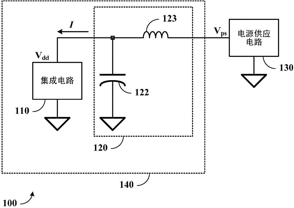
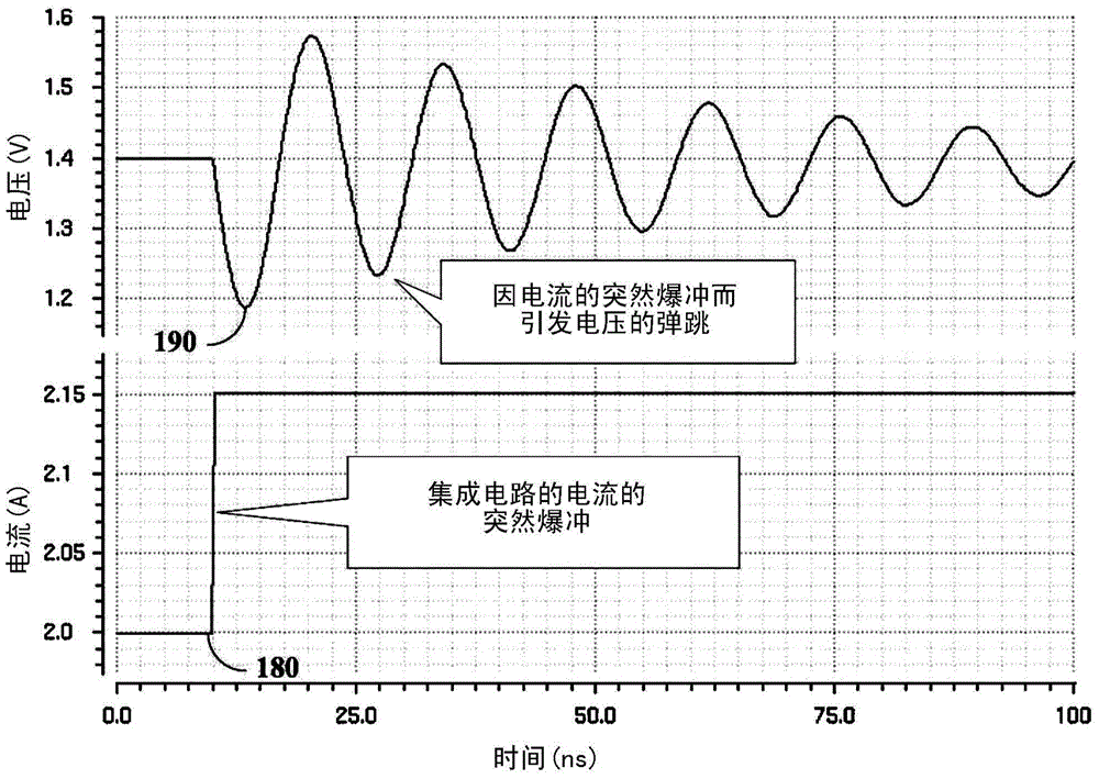
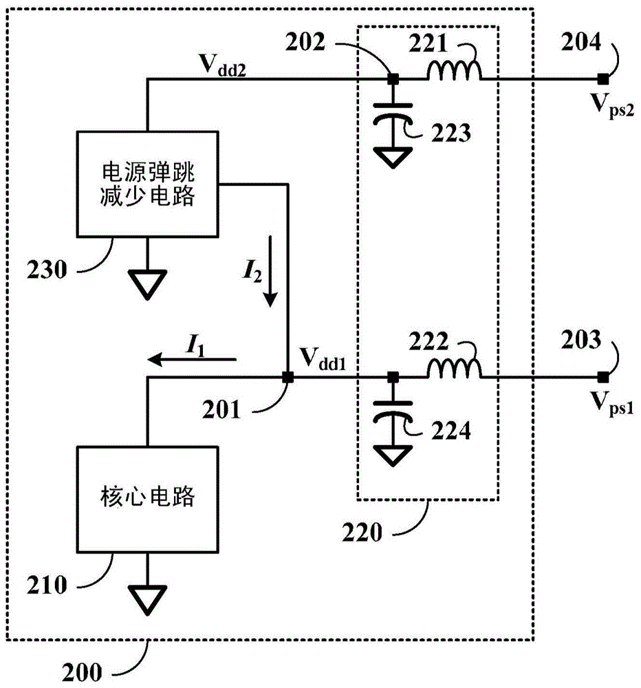
[0090] refer to figure 2 A packaged integrated circuit (IC) device 200 includes a core circuit 210 , a packaged circuit 220 and a power bounce reduction circuit 230 . The core circuit 210 is coupled to the first external power supply node 203 through the packaging circuit 220 . Here, the encapsulation circuit 220 is coupled between the first external power supply node 203 and the first internal power supply node 201 , and the core circuit 210 a...


PUM


Abstract

The invention discloses a packaging type integrated circuit component. A circuit is provided having a core circuit for sinking a first current from a first internal power supply node, a power bouncing reduction circuit for receiving power from a second internal power supply node and sourcing a second current to the first internal power supply node in accordance with a change of voltage at the first internal power supply node, and a package for coupling the first internal power supply node and the second internal power supply node to a first external power supply node and a second external power supply node, respectively. A corresponding method is also provided.

Description

technical field [0001] The invention relates to an integrated circuit, in particular to a packaged integrated circuit element and a method for reducing power supply bounce. Background technique [0002] Those skilled in the art should understand the various terms and basic concepts related to microelectronics used in the description, such as: P-type metal-oxide semiconductor (p-channelmetal-oxide semiconductor; PMOS), N-type metal-oxide semiconductor (n -channelmetal-oxide semiconductor; NMOS), "inductance", "capacitance", "resistance", "voltage", "current", "circuit node", "inverting amplifier (inverting amplifier)", "non-inverting amplifier (non- invertingamplifier)", "negative feedback", "source follower", "class-AB output stage (class-ABoutputstage)", "high-pass filter" and "biasing (biasing)". These terms and basic concepts can be obvious from prior art documents such as textbooks, so they will not be defined or explained in the specification. Among them, the textbook...

Claims


Application Information

Patent Timeline
Patent Type & Authority Applications(China)
IPC IPC(8): H03K19/00H03K19/003
CPCH03K17/165H03K2217/0027H03K2217/0063H03K2217/0081H03K17/162
Inventor 林嘉亮
Owner REALTEK SEMICON CORP
Why Eureka
Try Eureka