Device and method for generating single-layer and/or dual-layer plasma photonic crystal

A plasma and photonic crystal technology, applied in the field of plasma application technology and optics, can solve the problem that the device can only produce single-layer plasma photonic crystals and only double-layer plasma photonic crystals, etc. Effect

Inactive Publication Date: 2016-02-10
HEBEI UNIVERSITY
View PDF7 Cites 9 Cited by
  • Summary
  • Abstract
  • Description
  • Claims
  • Application Information

AI Technical Summary

Problems solved by technology

[0005] One of the purposes of the present invention is to provide a device for producing single-layer and/or double-layer plasmonic photonic crystals, to overcome the problem that existing devices can only produce single-layer plasmonic photonic c

Method used


Image

  • Device and method for generating single-layer and/or dual-layer plasma photonic crystal
  • Device and method for generating single-layer and/or dual-layer plasma photonic crystal
  • Device and method for generating single-layer and/or dual-layer plasma photonic crystal

Examples


Embodiment 1

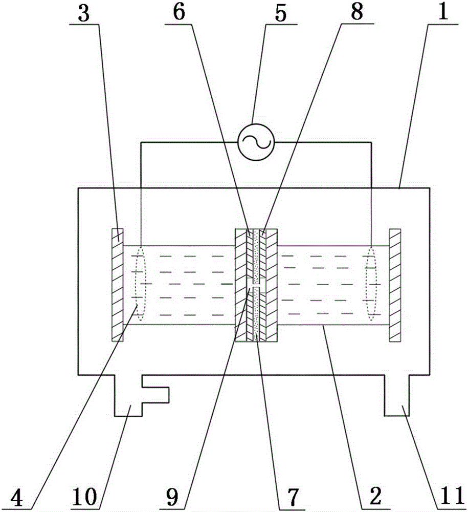
[0034] Such as figure 1 As shown, the device for producing single-layer and / or double-layer plasmonic photonic crystals provided by the present invention is to arrange two airtight dielectric containers symmetrically in a horizontal cylindrical vacuum reaction chamber 1, and in the airtight dielectric container Water is injected to form two water electrodes 2 . The two water electrodes 2 are electrically connected to a plasma generating power source 5 . The water electrode 2 is made of a plexiglass tube which is sealed by glass baffles 3 at both ends. The plexiglass tube is filled with water, and a copper ring 4 is set in the plexiglass tube. The two copper rings 4 are respectively electrically connected to the positive pole and the negative pole of the plasma generation power supply 5 outside the vacuum reaction chamber 1 through power lines. The thickness of the glass block 3 is between 0.5 mm and 3 mm.

[0035] Between the two water electrodes 2, there are left, middle a...

Embodiment 2

[0043] The method for producing single-layer and / or double-layer plasmonic photonic crystal provided by the present invention comprises the following steps:

[0044] a. A vacuum reaction chamber 1 is provided, an air inlet 10 and an air outlet 11 are provided on the wall of the vacuum reaction chamber 1 , and two water electrodes 2 are installed in the vacuum reaction chamber 1 . The water electrode 2 adopts a plexiglass tube sealed with glass baffles 3 on both sides and filled with water, and a built-in copper ring 4 is electrically connected to the plasma generating power supply 5 .

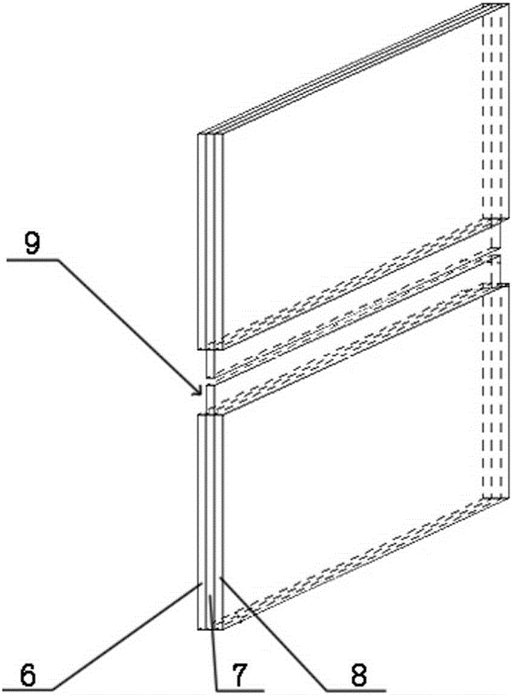
[0045] b. Between the two water electrodes 2, three layers of left, middle and right layers of glass are sequentially stacked and laminated. On the three layers of glass, a discharge gap 9 with a cavity cross-section in an H-shaped structure is formed, and the left, middle, and The three layers of glass on the right are perpendicular to the axis lines of the two water electrodes 2 respectively....

Embodiment 3

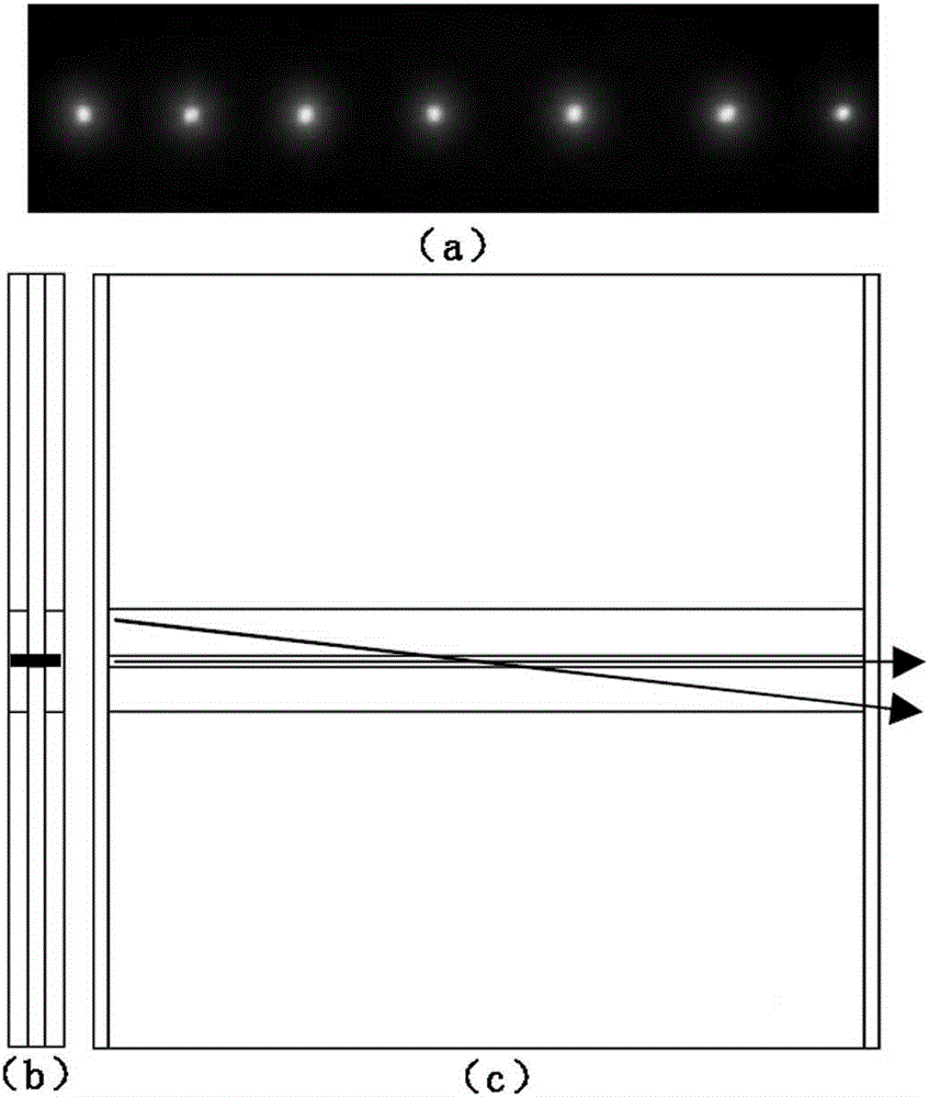
[0050] The present embodiment is compared with embodiment 2, and concrete experimental parameter is: the structure of three layers of glass is figure 2 In the structure shown, the thickness of the three layers of glass is 1.4mm; the length of the gap between the upper and lower glass in the left glass layer 6 is 80mm, and the width (that is, the distance between the upper and lower glass, or height) is 9mm The length of the gap between the upper and lower two sheets of glass in the middle glass layer 7 is 80mm, and the width is 1mm; the length of the gap between the upper and lower two sheets of glass in the right side glass layer 8 is 80mm, and the width is 9mm. The height of the single air gap in the middle of the discharge gap 9 is 1 mm, and the thickness is 4.2 mm (that is, the sum of the thicknesses of the three layers of glass). The upper and lower sides of the single air gap are double air gaps. For the double air gap on either side, the height of the two symmetrically...


PUM

PropertyMeasurementUnit
Thicknessaaaaaaaaaa
Thicknessaaaaaaaaaa
Thicknessaaaaaaaaaa

Abstract

The invention provides a device and method for generating a single-layer and/or dual-layer plasma photonic crystal. The device comprises a vacuum reaction chamber, two water electrodes and a plasma generation power supply, wherein the two water electrodes are installed in the vacuum reaction chamber; the plasma generation power supply is electrically connected with the water electrodes; a discharge gap with an empty cavity the cross section of which is of an H-type structure is formed between the two water electrodes via left, middle and right layers of sequentially overlapped and fit glass; and the left, middle and right layers of glass are respectively perpendicular to shaft axes of the two water electrodes. By the device provided by the invention, in combination with the method provided by the method, a single-layer photonic crystal, a two-layer photonic crystal or single-layer and dual-layer coexisting plasma photonic crystals can be generated in the discharge gap, so that the selection mode for modulating light is increased; moreover, single-air-gap slit plasma photonic crystals with multiple structures and types are realized for the first time. According to the invention, the wave band for modulating light beams is widened, and the diversification, convenience and high efficiency for light beam modulation are realized.

Description

technical field [0001] The invention relates to a plasma application technology and an optical technology, in particular to a device and method for producing single-layer and / or double-layer plasma photonic crystals. Background technique [0002] Photonic crystals, also known as photonic bandgap materials, are an artificial "crystal" structure formed by arranging two dielectric materials with different dielectric constants in space at a certain period (the size is on the order of the wavelength of light). The dielectric constant of a photonic crystal is a periodic function of space. If the periodic modulation of photons by the dielectric coefficient is strong enough, the photon energy propagating in the photonic crystal will also have an energy band structure, and photon "forbidden" will appear between the bands. band", photons whose frequency falls in the forbidden band cannot propagate in the crystal. The position and shape of the photonic forbidden band depend on the ref...

Claims


Application Information

Patent Timeline
IPC IPC(8): G02B1/00H05H1/24
CPCG02B1/005H05H1/2406
Inventor 董丽芳高星
Owner HEBEI UNIVERSITY
Why Eureka
Try Eureka