Screened film and preparation method thereof

A manufacturing method and technology of shielding film, which are applied in the fields of magnetic field/electric field shielding, electrical components, etc., can solve the problems of reducing the shielding effect of the shielding film 1, large contact resistance, and poor conductivity.

Active Publication Date: 2016-02-10
APLUS SEMICON TECH CO LTD
View PDF7 Cites 8 Cited by
  • Summary
  • Abstract
  • Description
  • Claims
  • Application Information

AI Technical Summary

Problems solved by technology

[0008] However, if figure 1 The existing structure of the shielding film 1 shown above is due to the addition of conductive particles 13a in the conductive adhesive layer 13. Although this structure can achieve the functions of adhesion and conduction, the contact resistance between the conductive particles

Method used


Image

  • Screened film and preparation method thereof
  • Screened film and preparation method thereof
  • Screened film and preparation method thereof

Examples


no. 1 example

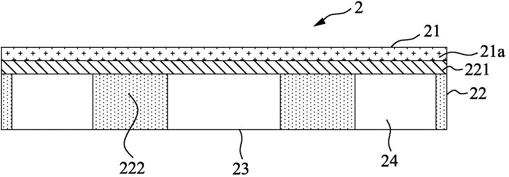
[0063] see Figure 2A , which is the first embodiment of the shielding film 2 structure of the present invention, which includes: an insulating layer 21 , at least one conductive shielding layer 22 and an adhesive layer 24 .

[0064] Such as Figure 2A As shown, the insulating layer 21 may be a separate structure having a first insulating material 21a, and the thickness of the first insulating material 21a is between 5 and 25 microns. The material of the first insulating material 21a can be selected from polyimide (PI-Polyimide), polyethylene terephthalate (PET-Polyethylene Terephthalate), polycarbonate (PC-polycarbonate) or polyphenylsulfone ( PPSU-Polyphenylensulfon) at least one of the materials. In a preferred embodiment, the above-mentioned first insulating material 21a is made of a black material, which has a better effect when manufacturing the shielding film 2 of the present invention.

[0065] read on Figure 2A As shown, a conductive shielding layer 22 is arrange...

no. 4 example

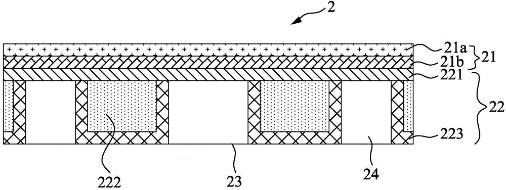
[0106] see Figure 16-17 It is a fourth embodiment of a manufacturing method of a shielding film 2, which includes the following steps:

[0107] (A) providing an insulating layer 21;

[0108] (B) forming a conductive shielding layer 22 on the surface of the insulating layer 21 by evaporation, sputtering or chemical plating;

[0109] (C) Simultaneous die-casting of the above-mentioned insulating layer 21 and the conductive shielding layer 22 with an embossing machine to jointly form a raised metal ground electrode 222;

[0110] (D) An adhesive layer 24 is filled in the filling space 23 on the surface of the conductive shielding layer 22 , and the metal ground electrode 222 is exposed on the surface to form a scattered pattern.

[0111] see Figure 18-19 It is a schematic flow chart of a fifth embodiment of a manufacturing method of a shielding film 2 and a structural diagram thereof, which includes the following steps:

[0112] The step (A) is to first provide a first insul...


PUM

PropertyMeasurementUnit
Thicknessaaaaaaaaaa
Heightaaaaaaaaaa
Thicknessaaaaaaaaaa

Abstract

The invention relates to a screened film and a preparation method thereof. The screened film structurally comprises an insulating layer, a conductive shielding layer and an adhesive layer. The preparation method of the screened film comprises that (A) a base material and the conductive shielding layer are connected and the form recesses; (B) the insulating layer is formed at the surface of the conductive shielding layer and filled into the recesses; (C) a carrier film is formed at the surface of the insulating layer; (D) the base material is removed; and (E) the surface of the conductive shielding layer is provided with the adhesive layer, and a metal grounding electrode is exposed to form a distribution pattern. According to the structure and preparation method of the screened film, the screened film is good in grounding effect and high in adhesion intensity, the electromagnetic shielding effect is indirectly improved, and the preparation method is characterized by reducing the cost and simplifying the process.

Description

technical field [0001] The invention relates to a shielding film structure and a manufacturing method thereof, in particular to a shielding film structure and a manufacturing method thereof which increase the grounding performance of the shielding film and further enhance electromagnetic shielding benefits. Background technique [0002] In response to the current development needs of electronic and communication products, the current industry requires light, thin, short, and small product structures, and high performance in terms of functions. [0003] However, in order to achieve the above goals, the circuits of electronic products are often dense and the frequency is high, making the problem of electromagnetic radiation more and more serious, causing interference between devices, and even affecting human health. [0004] In the past, in order to solve the problem of electromagnetic radiation, it was only necessary to rely on the special design and planning of the circuit, ...

Claims


Application Information

Patent Timeline
IPC IPC(8): H05K9/00
Inventor 赖玉豪
Owner APLUS SEMICON TECH CO LTD
Why Eureka
Try Eureka