Wavelength division multiplex light receiving assembly

A wavelength-division multiplexing and wavelength-division multiplexing technology, applied in the field of optical communication, can solve problems such as the manifestation of advantages and complex optical path structure, and achieve the effects of increasing stability and reliability, simplifying optical path structure, and reducing packaging difficulty.

Active Publication Date: 2016-02-17
GUANGXUN SCI & TECH WUHAN
View PDF7 Cites 19 Cited by
  • Summary
  • Abstract
  • Description
  • Claims
  • Application Information

AI Technical Summary

Problems solved by technology

[0006] To sum up, the existing wavelength division multiplexing optical receiving components use spatial optical filters to realize wavelength demultiplexing; components such as optical input ports and lenses are used as optical input channels, resulting in an extremely complex optical path structure, which is very difficult for packaging. Craftsmanship poses great challenges
However, the advantages of the existing planar optical waveguide integrated wavelength division multiplexing chip and optical fiber components are not reflected in the wavelength division multiplexing optical receiving components

Method used


Image

  • Wavelength division multiplex light receiving assembly
  • Wavelength division multiplex light receiving assembly
  • Wavelength division multiplex light receiving assembly

Examples


Embodiment 1

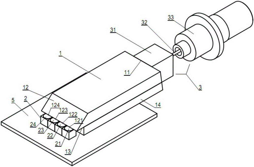
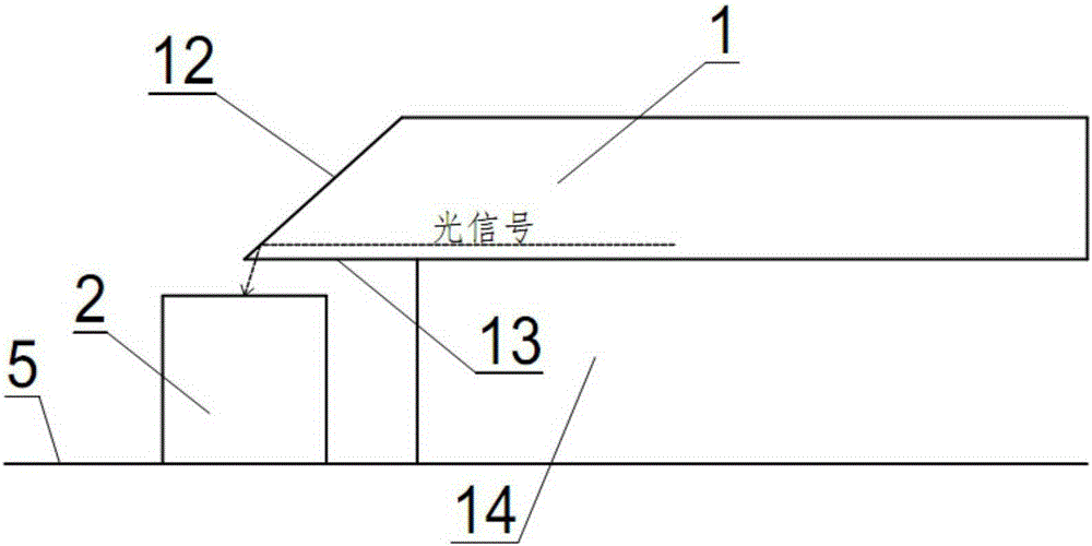
[0046] Such as Figure 4 As shown, a planar optical waveguide integrated wavelength division multiplexing chip 1 , a photodetector array chip 2 , and an optical fiber assembly 3 are arranged in a packaging case 4 . The input end surface 11 of the planar optical waveguide integrated wavelength division multiplexing chip is the same polished surface as the coupling port of the optical fiber component, and is glued together with the coupling port 31 of the optical fiber component. The output end surface 12 of the planar optical waveguide integrated wavelength division multiplexing chip is an uncoated polished surface, which forms an angle of 40° with the waveguide surface 13, and the light in the output waveguide is totally reflected on the output end surface 12 and enters the photodetector. The photodetector chip array 2 is located on the reflective light path below the output end surface 12 of the planar optical waveguide integrated wavelength division multiplexing chip. There ...

Embodiment 2

[0049] Such as Figure 5As shown, a planar optical waveguide integrated wavelength division multiplexing chip 1 , a photodetector array chip 2 , and an optical fiber assembly 3 are arranged in a packaging case 4 . The input end surface 11 of the planar optical waveguide integrated wavelength division multiplexing chip is the same polished surface as the coupling port of the optical fiber component, and is glued together with the coupling port 31 of the optical fiber component. The output end face 12 of the planar optical waveguide integrated wavelength division multiplexing chip is polished and forms a 50° angle with the waveguide surface 13. The output end face 12 of the planar optical waveguide integrated wavelength division multiplexing chip is also coated with a reflective film. The reflectivity of light on this surface is greater than 80%. The photodetector chip array 2 is located on the reflective light path below the output end surface 12 of the planar optical waveguid...


PUM


Abstract

The invention discloses a wavelength division multiplex light receiving assembly. The wavelength division multiplex light receiving assembly comprises a plane light waveguide integrated wavelength division multiplex chip (1), a light detector chip array (2) and an optical fiber assembly (3), wherein a coupling port (31) of the optical fiber assembly (3) is coupled and stuck with an input end of the plane light waveguide integrated wavelength division multiplex chip (1); the light detector chip array (2) is located under an output end face (12) of the plane light waveguide integrated wavelength division multiplex chip; light sensitive faces (21, 22, 23, 24...) of the light detector chip array are correspondingly aligned with output waveguides (121, 122, 123, 124...) of the plane light waveguide integrated wavelength division multiplex chip (1); and an included angle of 40-50 degrees is formed between the output end face (12) of the plane light waveguide integrated wavelength division multiplex chip and a waveguide face (13), so that the output end face (12) can be used for outputting light reflection parallel to the waveguide face (13) from the waveguide face to be coupled with the light sensitive faces of the light detector chip array. According to the wavelength division multiplex light receiving assembly, the solution multiplexing of a light signal is finished by the plane light waveguide integrated wavelength division multiplex chip and the output end face of the plane light waveguide integrated wavelength division multiplex chip is used as a light reflection face, so that the optical fiber assembly is used as a light input channel. According to the wavelength division multiplex light receiving assembly, a light path structure is extremely simplified, the stability of a light path is enhanced and the coupling packaging difficulty is reduced, so that the integration and low cost of the wavelength division multiplex light receiving assembly are realized.

Description

technical field [0001] The invention relates to an optical receiving component, in particular to a wavelength division multiplexing optical receiving component, and belongs to the field of optical communication. Background technique [0002] Data centers and high-performance computing applications place increasingly stringent requirements on the transmission rate and package size of optical components. In response to this demand, the IEEE organization has specially formulated the IEEE802.ba specification, which specifies the 40G and 100G Ethernet transmission standards. Using CWDM / Lan-WDM wavelength division multiplexing technology to achieve 40G / 100G transmission rate and optical components that meet specific package sizes is a huge challenge in the current optical communication field. [0003] The optical path structure of the existing CWDM / Lan-WDM wavelength division multiplexing optical receiving components is mostly: after the light enters the input port, it is collima...

Claims


Application Information

Patent Timeline
Patent Type & Authority Applications(China)
IPC IPC(8): G02B6/293G02B6/42H04B10/67
CPCG02B6/29301G02B6/4215G02B6/4286H04B10/67
Inventor 朱虎翟宇佳成璇璇陈沛马卫东
Owner GUANGXUN SCI & TECH WUHAN
Why Eureka
Try Eureka