Formation method for fin type field-effect transistor
A fin-type field effect transistor and fin technology are applied in the direction of electrical components, semiconductor/solid-state device manufacturing, circuits, etc., which can solve the problem that the electrical performance of the fin-type field effect transistor needs to be improved, and achieve improved electrical performance and reliability. The effect of avoiding etching and maintaining integrity
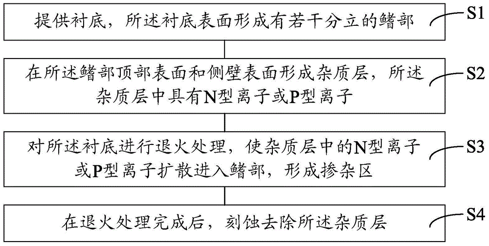
- Summary
- Abstract
- Description
- Claims
- Application Information
AI Technical Summary
Problems solved by technology
Method used
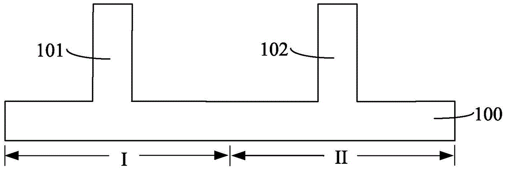
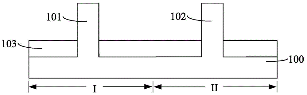
Image

Examples
Embodiment Construction
[0034] It can be seen from the background art that the electrical performance of the fin field effect transistor formed in the prior art needs to be improved.
[0035] After research, it is found that in the prior art, when the source region and the drain region of the FinFET are used, the method of ion implantation is usually used to dope the fin of the FinFET; since the fin is a three-dimensional structure, the ion implantation When the angle is different, the concentration and implantation depth of ion implantation in the source region and the drain region will be different, resulting in the problem of non-conformal doping. The doping concentration of each region of the fin is different, for example, the top region of the fin The doping concentration of the doping concentration is higher than that of the sidewall region of the fin; the non-conformal doping problem is an important reason for the poor electrical performance of the FinFET.
[0036] Moreover, the ion implantati...
PUM
 Abstract
Description
Claims
Application Information
 - R&D
- Intellectual Property
- Life Sciences
- Materials
- Tech Scout
- Unparalleled Data Quality
- Higher Quality Content
- 60% Fewer Hallucinations
Browse by: Latest US Patents, China's latest patents, Technical Efficacy Thesaurus, Application Domain, Technology Topic, Popular Technical Reports.
© 2025 PatSnap. All rights reserved.Legal|Privacy policy|Modern Slavery Act Transparency Statement|Sitemap|About US| Contact US: help@patsnap.com