Protective tape and semiconductor device manufacturing method using same
A protective tape and base material technology, which is applied in semiconductor/solid-state device manufacturing, semiconductor devices, semiconductor/solid-state device components, etc., can solve problems such as reducing connectivity and hindering welding, and achieve excellent connectivity.
- Summary
- Abstract
- Description
- Claims
- Application Information
AI Technical Summary
Problems solved by technology
Method used
Image
Examples
Embodiment
[0074]
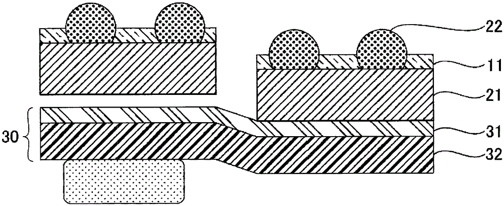
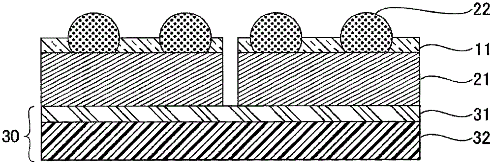
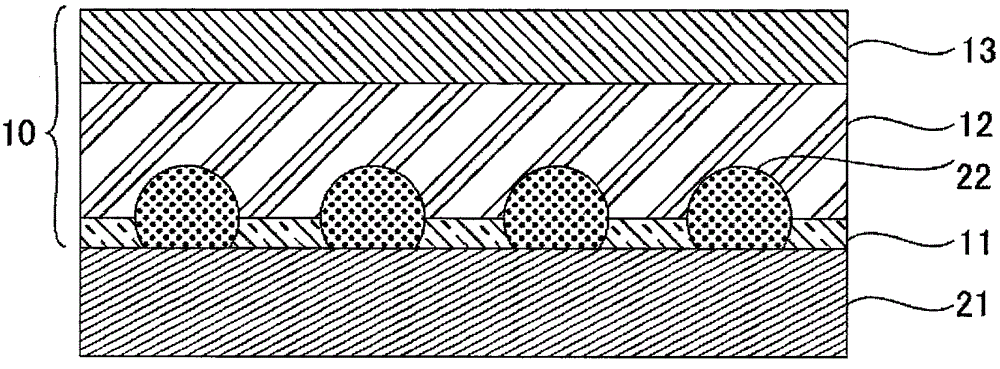
[0075] Hereinafter, examples of the present invention will be described. In this example, a protective tape in which an adhesive layer and a thermoplastic resin layer were laminated was fabricated. Use the protective tape, and sequentially perform the protective tape sticking process (A), grinding process (B), adhesive tape sticking process (C), protective tape peeling process (D), curing process (E), cutting treatment process (F), The expansion process (G), the pick-up process (H) and the mounting process (I), thereby producing a semiconductor device. Furthermore, the solderability and bump embedding properties of the semiconductor device were evaluated. In addition, the present invention is not limited to these Examples.
[0076] [Making of protective tape]
[0077] As shown in Table 1, adhesive bond layers A1 to A3 were prepared. Adhesive layer A1 was prepared by mixing 13.0 parts by mass of film-forming resin, 54.8 parts by mass of epoxy resin, 32.4 parts by...
Embodiment 2
[0103] As shown in Table 2, the adhesive layer A2 and the thermoplastic resin layer B3 were laminated, and the protective tape whose elastic modulus ratio of the adhesive layer and the thermoplastic resin layer was 2.1E-03 was produced. Using this protective tape, a semiconductor device was produced by the above-mentioned method. At this time, the evaluation of solderability was 85%, and the evaluation of bump embedding property was "Δ".
Embodiment 3
[0105] As shown in Table 2, the adhesive layer A3 and the thermoplastic resin layer B1 were laminated, and a protective tape having an elastic modulus ratio of the adhesive layer and the thermoplastic resin layer of 3.0E-05 was produced. Using this protective tape, a semiconductor device was produced by the above-mentioned method. At this time, the evaluation of solderability was 110%, and the evaluation of bump embedding property was "◯".
[0106]
[0107] As shown in Table 2, the adhesive layer A1 and the thermoplastic resin layer B2 were laminated, and the protective tape whose elastic modulus ratio of the adhesive layer and the thermoplastic resin layer was 2.4E-02 was produced. Using this protective tape, a semiconductor device was produced by the above-mentioned method, and the evaluation of solderability at this time was 12%.
[0108]
[0109] As shown in Table 2, the adhesive layer A2 and the thermoplastic resin layer B1 were laminated, and a protective tape having...
PUM
 Abstract
Description
Claims
Application Information
 - R&D
- Intellectual Property
- Life Sciences
- Materials
- Tech Scout
- Unparalleled Data Quality
- Higher Quality Content
- 60% Fewer Hallucinations
Browse by: Latest US Patents, China's latest patents, Technical Efficacy Thesaurus, Application Domain, Technology Topic, Popular Technical Reports.
© 2025 PatSnap. All rights reserved.Legal|Privacy policy|Modern Slavery Act Transparency Statement|Sitemap|About US| Contact US: help@patsnap.com


