A hybrid memory hardware implementation system and method

A hardware-implemented, mixed-memory technology, applied in the field of memory, to achieve the effect of improving the refresh cycle and reducing refresh power consumption

Active Publication Date: 2018-06-29
SHANGHAI XINCHU INTEGRATED CIRCUIT
View PDF4 Cites 0 Cited by
  • Summary
  • Abstract
  • Description
  • Claims
  • Application Information

AI Technical Summary

Problems solved by technology

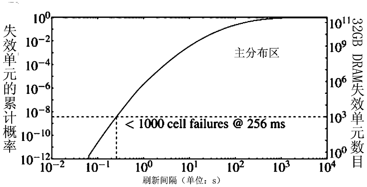
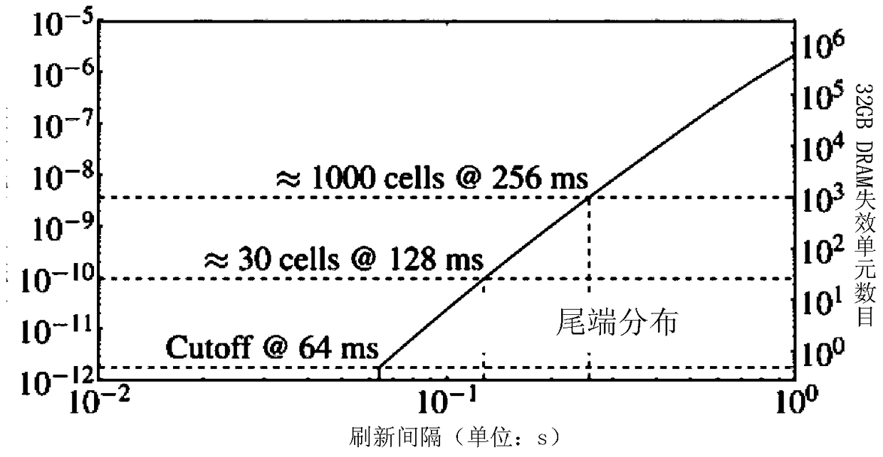
It can be seen from the figure that the holding time of most storage units can reach 1s or even longer, while less than 1% of the storage units are distributed at the tail end, and their holding time is lower than 1s or even less than 100ms
[0005] There are still many problems unsolved in this technical solution. For example, when the memory controller requests data from the hybrid memory, it sends an address to the hybrid memory. How does the hybrid memory determine whether the data corresponding to the address is stored in the NCM or in the NCM? In DRAM, how the physical address of NCM and the physical address of DRAM are mapped, this is the technical loophole of adding NCM storage

Method used


Image

  • A hybrid memory hardware implementation system and method
  • A hybrid memory hardware implementation system and method
  • A hybrid memory hardware implementation system and method

Examples


Embodiment 1

[0050] Figure 4a-4b It is a schematic diagram of Embodiment 1 of the two hybrid memory structures in this embodiment, and this embodiment proposes a specific hardware implementation of the hybrid memory. The hybrid memory of this embodiment includes a traditional DRAM storage area and a new memory (NCM) area, and the minimum access bit width of the DRAM storage area and the NCM storage area should be consistent. For example, a read operation of the DRAM can currently read If 64-bit data is output, then a read operation to NCM should also read 64-bit data. General memory is composed of multiple DRAM chips so that it can be processed in parallel, speeding up DRAM access speed and increasing data bandwidth.

[0051]Hybrid memory has two structures: the first one is only one NCM memory chip, if attached Figure 4a As shown, assuming that the data bit width of a single DRAM chip is n, and the number of DRAM chips is N, then the total data bit width M of the DRAM is n*N, and the ...

Embodiment 2

[0081] Figure 7 It is a schematic diagram of Embodiment 2 of a hardware implementation method of a hybrid memory in this embodiment, a hardware implementation method of a hybrid memory, and the hardware implementation method includes:

[0082] Step S1: sending data requests to the DRAM memory and the address lookup conversion module respectively;

[0083] Step S2: The address lookup conversion module receives the physical address of the data request, and judges whether the physical address of the requested data exists in the DRAM address list in the address lookup conversion module; if so, then execute step S3, if not, then execute step S4.

[0084] Step S3: The control module generates a control signal and sends it to the multiplexer. The multiplexer selects the data in the NCM memory for output according to the control signal, and sends the NCM physical address corresponding to the matching DRAM address to the NCM memory.

[0085]Step S4: the control module outputs the dat...


PUM


Abstract

The invention relates to the field of a memorizer, and in particular to a hardware implementation system and method for a hybrid memory. The hybrid memory at least comprises N DRAM memorizers, at least an NCM memorizer, an address lookup conversion module, a control module and a multiplexer, wherein the N DRAM memorizers are divided into a main distributing region and a tail end distributing region according to DRAM storage unit retention time; N is an integer; the at least one NCM memorizer can substitute the DRAM memorizers to store the storage data in the tail end distributing region of the DRAM memorizers; the address information of the storage data in the tail end distributing region in the DRAM memorizers and the corresponding address information in the NCM memorizer for substituting the DRAM memorizers to store the storage data in the tail end distributing region in the DRAM memorizers are pre-stored in the address lookup conversion module; the control module is used for obtaining address information and address mapping relation, and judging the output access source of the system data according to the address information and address mapping relation, and the control module generates and outputs a control signal according to the source of the output access; and the multiplexer is connected with the control module, the DRAM memorizers and the NCM memorizer separately for receiving the control signal and selecting data for outputting according to the control signal.

Description

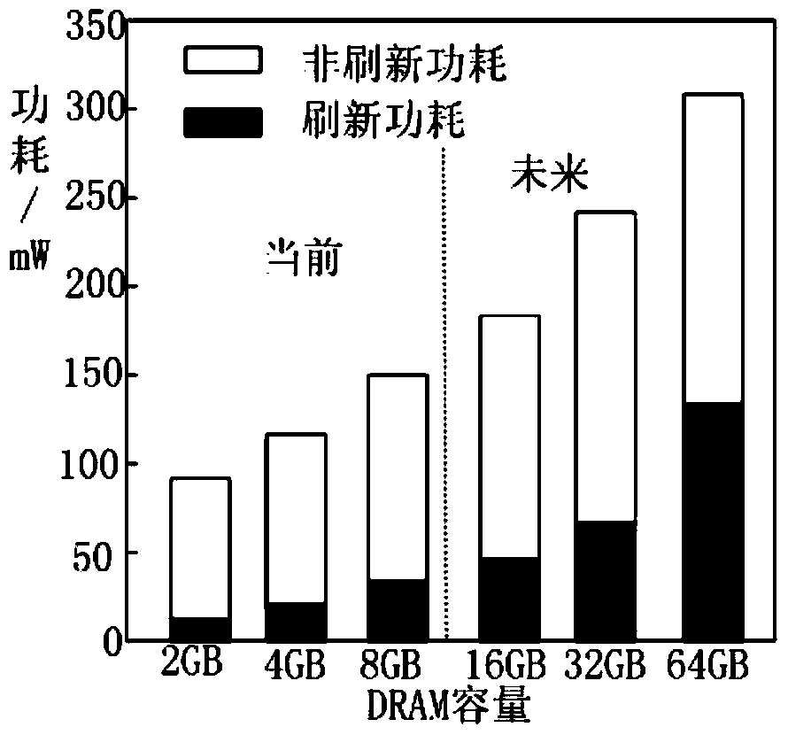
technical field [0001] The invention relates to the field of memory, in particular to a hardware implementation system and method of a hybrid memory. Background technique [0002] In the past few decades, the cost of DRAM (Dynamic Random Access Memory, DRAM) has been continuously reduced along with Moore's Law. However, as the feature size becomes smaller and smaller, the chip has higher and higher requirements for power consumption. Due to the leakage of DRAM storage capacitors, it must be refreshed every once in a while, and the refresh power consumption is getting larger and larger. figure 1 It is a schematic diagram of the proportion and trend of DRAM refresh power consumption in the prior art, such as figure 1 As shown, the DRAM refresh power consumption further increases with the increase of the DRAM capacity. The refresh cycle of a DRAM is determined by the retention time of charges in its memory cells. [0003] Figure 2a-2b It is a schematic diagram of DRAM rete...

Claims


Application Information

Patent Timeline
Patent Type & Authority Patents(China)
IPC IPC(8): G06F3/06
CPCG06F3/0625G06F3/0685
Inventor 景蔚亮叶勇
Owner SHANGHAI XINCHU INTEGRATED CIRCUIT
Why Eureka
Try Eureka