Apparatus for achieving in-situ micromechanics, microstructure and component integrated research in scanning electron microscope

A micromechanics, scanning mirror technology, applied in scanning probe technology, instruments, etc., can solve problems such as inability to deepen scientific problems, incompatibility with signal acquisition, inability to perform real-time in-situ measurement and characterization, and achieve compact structure and design. Compact structure and small volume effect

CN105388327AActive Publication Date: 2016-03-09浙江祺跃科技有限公司
9 Cites 31 Cited by

Patent Information

Authority / Receiving Office
CN · China
Current Assignee / Owner
Publication Date
2016-03-09

Smart Images

  • Figure 1
    Figure 1
  • Figure 2
    Figure 2
  • Figure 3
    Figure 3
Patent Text Reader

Abstract

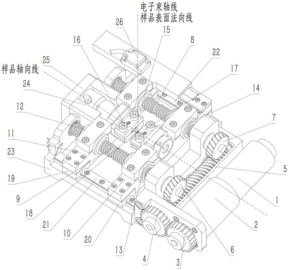
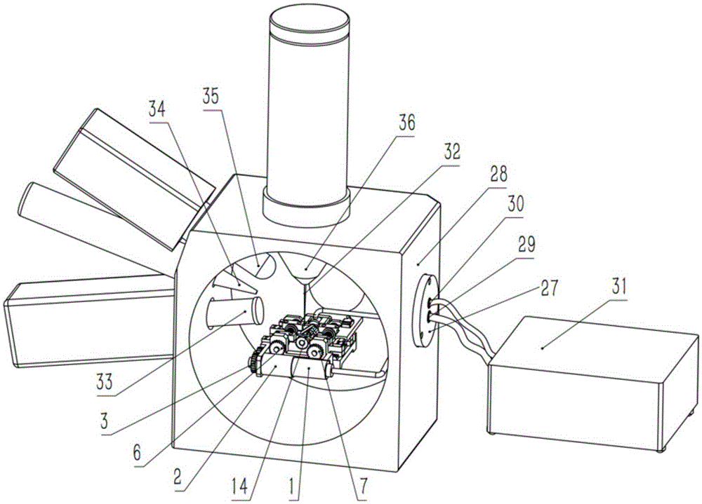
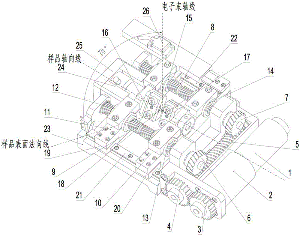
An apparatus for achieving in-situ micromechanics, microstructure and component integrated research in a scanning electron microscope belongs to the field of material microstructure and performance in-situ characterization. According to the apparatus, a double trapezoid leading screw transmission system is adopted, thus the apparatus is large in rigidity and high in test precision; the apparatus can stably operate in the scanning electron microscope, has low mechanical noise, and has low interference on scanning electron microscope imaging; the trapezoid leading screw has a self-locking function, thus the test can be paused and started at any time, continuity of test data is good; a sample clamp has a rotation function, thus when material extension / compression mechanical properties are measured, scanning electron beam imaging, EDS and EBSD integrated test can be satisfied at the same micro area; clamp support frames designed by the apparatus, the sample clamps and samples have the completely symmetrical structure, thus the samples receive the completely symmetrical extension / compression stress, and a geometric center of the sample, i.e., a deformation center, is located right under an electron beam all the time, thereby facilitating in-situ tracking dynamic research and high-quality microscopic scanning image acquisition.
Need to check novelty before this filing date? Find Prior Art

Description

Technical field:

[0001] The invention relates to a device for in-situ micromechanics, microstructure and component integration research in a scanning electron microscope, which belongs to the field of in-situ characterization of material microstructure and performance. Background technique

[0002] Regardless of whether it is a functional material or a structural material, the microstructure and composition information that make up these materials are the decisive factors that determine the physical and mechanical properties of the material. However, for a long time, the measurement of mechanical properties of materials and the characterization of microstructure and composition distribution have been carried out independently. Even though there are a few mechanical experiments that can be carried out under diffraction conditions such as X-rays and synchrotron radiation, there is still a lack of in-situ, real-time, real-space high-resolution microstructural image information....

Examples

Embodiment Construction

[0030] The present invention will be further described below in conjunction with the accompanying drawings and specific embodiments.

[0031] A device for in-situ micromechanics, microstructure, and component integration research in a scanning electron microscope is designed based on FEIQuanta650 field emission environmental scanning electron microscope, FEIQuanta250 tungsten filament environmental scanning electron microscope and JEOLJSM6500F field emission scanning electron microscope. The length, width and height of the device are 140mm*110mm*45mm, which can be easily installed in the sample room of the scanning electron microscope. The load range is 0-2000N, the load accuracy is 0.1% FSO, the displacement stroke range is 0-25mm, and the displacement accuracy is 0.02um. The rate range is 0~40um / s. In the experiment, in the FEIQuanta250 tungsten filament environmental scanning electron microscope, the microscopic deformation process and the microscopic crack propagation proc...