Method for improving uniformity of PCB copper reduction

A technology of uniformity and PCB board, which is applied in the field of circuit board processing and manufacturing, can solve the problems of inability to control the uniformity of copper thickness, and achieve the effects of convenient operation, improved uniformity, and guaranteed thickness and uniformity

Active Publication Date: 2016-03-09
NEW FOUNDER HLDG DEV LLC +1
View PDF4 Cites 7 Cited by
  • Summary
  • Abstract
  • Description
  • Claims
  • Application Information

AI Technical Summary

Problems solved by technology

Although this scheme protects the hole copper, it still cannot control the uniformity of copper thickness after copper reduction

Method used


Image

  • Method for improving uniformity of PCB copper reduction
  • Method for improving uniformity of PCB copper reduction
  • Method for improving uniformity of PCB copper reduction

Examples


Embodiment

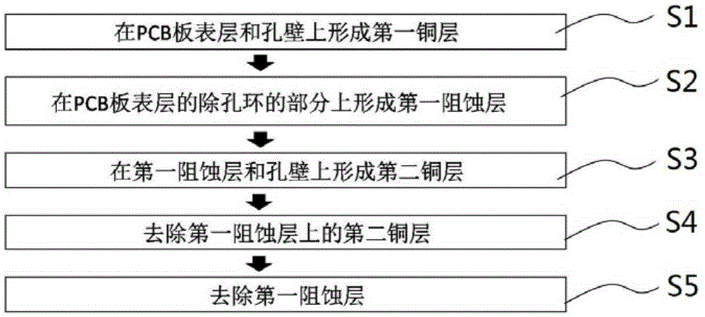
[0039] This embodiment provides a method for improving the uniformity of PCB copper reduction, such as figure 1 shown, including the following steps:

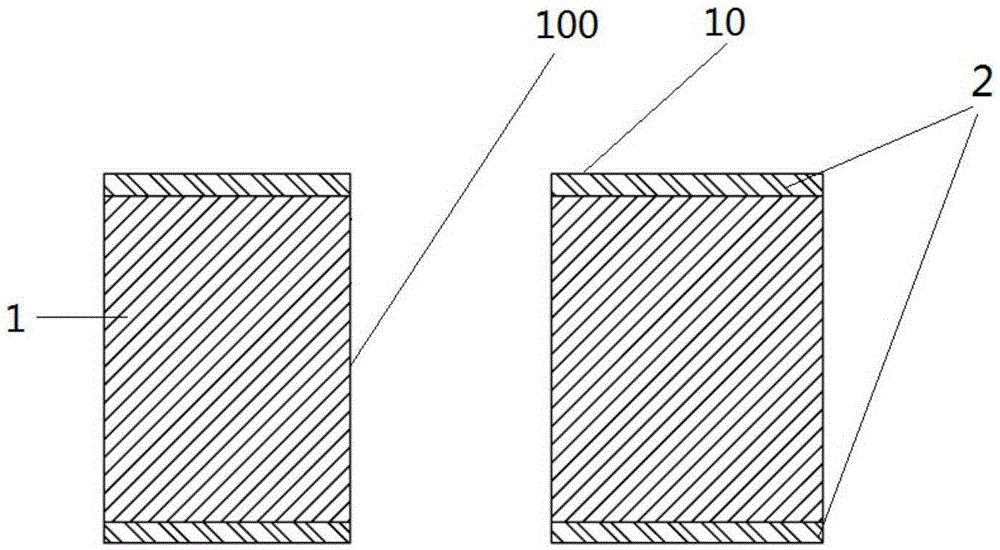
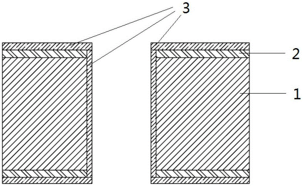
[0040] S1. Form the first copper layer 3 on the surface layer 10 of the PCB 1 and the wall 100 of the through hole. Among them, such as Figure 2a As shown, the PCB board 1 is provided with several through holes passing through it, the base copper layer 2 is formed on the surface layer 10 of the PCB board 1 , and the base copper layer 2 is not provided on the hole wall 100 of the through hole. After forming the first copper layer 3, such as Figure 2b As shown, the first copper layer 3 is directly formed on the base copper layer 2 and the hole wall 100 .

[0041] As a preferred embodiment of the present invention, the first copper layer 3 is prepared by an electroplating process; as an alternative embodiment of the present invention, the preparation method of the first copper layer 3 is not limited thereto, and can also be m...


PUM


Abstract

The invention discloses a method of improving the uniformity of PCB copper reduction. The method comprises the steps of forming a first copper layer on a surface layer of a PCB and a pore wall; forming an anti-corrosion layer on a portion, other than a pore ring, of the surface layer of the PCB; forming a second copper layer on the first anti-corrosion layer and the pore wall; removing the second copper layer on the first anti-corrosion layer; and removing the first anti-corrosion layer. In this way, the amount of copper reduction can be controlled by forming surface copper at a time, forming pore copper for a plurality of times, and forming the first anti-corrosion layer; the uniformity of the copper reduction is controlled by the etching of the first anti-corrosion layer; the thickness and uniformity of the surface copper are effectively ensured; and the method is convenient to operate and easy to implement.

Description

technical field [0001] The invention relates to the field of circuit board processing and manufacturing, in particular to a method for improving the uniformity of PCB copper reduction. Background technique [0002] With the rapid development of microelectronics technology, the level of PCB processing and manufacturing technology has been greatly improved, and large-scale or even ultra-large-scale integrated circuits are widely used. [0003] In the prior art, the hole wall metallization process of PCB is generally as follows: first, a thin layer of copper is formed on the hole wall by metal palladium catalysis, and then the copper thickness of the hole wall can be thickened by an electrochemical method. Then carry out graphic electroplating, and use the copper thickness of the hole wall and the surface copper thickness to meet the customer's requirements. Due to the deep plating ability of electroplating, the relationship between the growth of hole wall copper thickness and...

Claims


Application Information

Patent Timeline
Patent Type & Authority Applications(China)
IPC IPC(8): H05K3/18H05K3/42
CPCH05K3/18H05K3/425H05K2203/0369
Inventor 刘大辉
Owner NEW FOUNDER HLDG DEV LLC
Why Eureka
Try Eureka