A kind of oled screen body and preparation method thereof
An electrode layer and substrate technology, applied in the field of OLED, can solve the problems of reducing the efficiency roll-off and efficiency reduction of the screen body, and achieve the effects of improving the brightness, suppressing the efficiency roll-off, and improving the uniformity of light emission.
- Summary
- Abstract
- Description
- Claims
- Application Information
AI Technical Summary
Problems solved by technology
Method used
Image
Examples
Embodiment 1
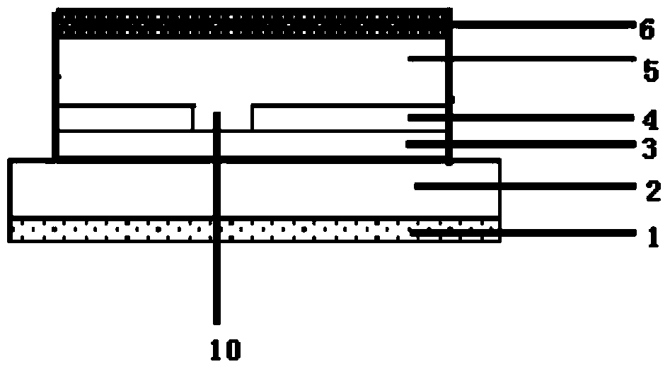
[0030] Embodiment 1 A scattering film layer 1 is arranged on the outside of the substrate
[0031] Such as figure 1 with Figure 4 As shown, a relatively bright OLED panel provided by the present invention includes a substrate 2 and a first electrode layer 3, an organic light-emitting layer 5 and a second electrode layer 6 are stacked on the substrate 2. An insulating film layer is arranged between an electrode layer 3 (anode) and the organic light-emitting layer 5, such as Figure 4 with Figure 5 As shown, the insulating film layer is etched to form parallel or criss-cross light-emitting regions 10, the width of each light-emitting region 10 is 5nm-500um, preferably 50nm-100um, between adjacent light-emitting regions 10 The width of the insulating material layer 4 is 10nm-100um. The thickness of the insulating film layer is 5-20nm. As other implementation manners, the insulating film layer may also be Image 6 with Figure 7 As shown, its light-emitting area is a para...
Embodiment 2
[0037] Embodiment 2 A scattering film layer 1 is arranged between the substrate and the first electrode layer
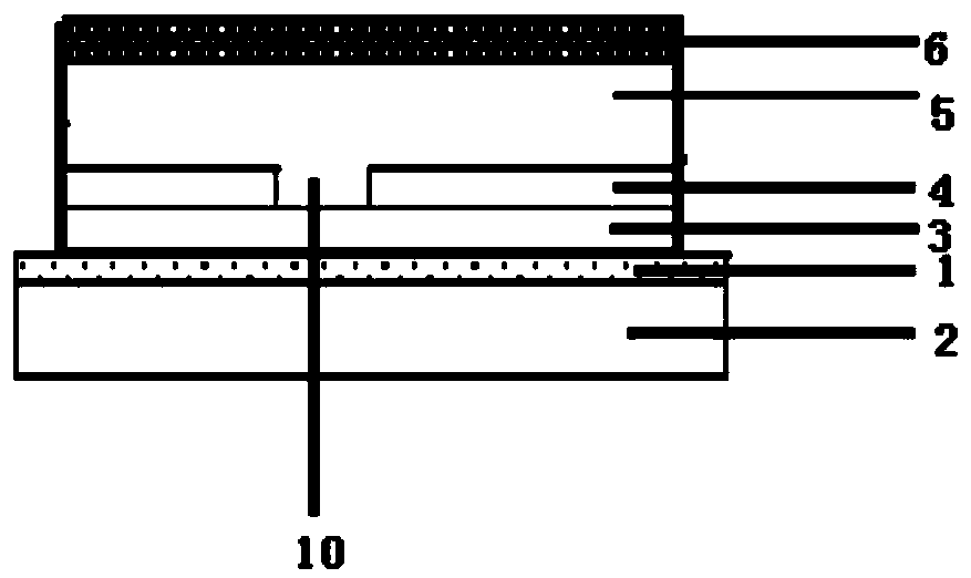
[0038] The structure of a relatively bright OLED screen body provided in this embodiment is the same as that in Embodiment 1, such as figure 2 As shown, the scattering film layer 1 is arranged between the substrate 2 and the first electrode layer 3 .
[0039]The preparation method is to arrange a scattering film layer 1 on the substrate 2, coat a layer of insulating film layer on the scattering film layer 1, and the width of the insulating material layer 4 between the adjacent light-emitting regions is 10nm-100um, and then pass the electron beam Photolithography technology carries out photoetching to etch out the light-emitting region 10, the width of the light-emitting region 10 is 5nm-500um, preferably the width is 50nm-100um, and then vapor-deposits the first electrode layer 3, the organic light-emitting layer 5 and the second electrode layer 6 ( cathode), packa...
Embodiment 3
[0040] Embodiment 3 The scattering film layer 1 is respectively arranged on both sides of the substrate
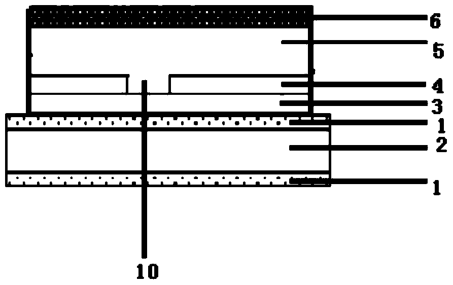
[0041] The structure of a relatively bright OLED screen body provided in this embodiment is the same as that in Embodiment 1, such as image 3 As shown, the two sides of the substrate are respectively provided with scattering film layers 1, that is, one of the scattering film layers 1 is provided between the substrate 2 and the first electrode layer 3, and the other scattering film layer 1 is provided between the The side of the substrate away from the first electrode layer.
[0042] The preparation method is as follows: setting an upper scattering film layer 1 on the substrate 2, coating a layer of insulating film layer on the scattering film layer 1, and then performing photolithography to etch a light-emitting region 10 by electron beam lithography technology. The width of the light-emitting region 10 is 5nm-500um, the preferred width is 50nm-100um, the width of the in...
PUM
 Abstract
Description
Claims
Application Information


