Displays with silicon and semiconducting oxide thin-film transistors
What is Al technical title?
Al technical title is built by PatSnap Al team. It summarizes the technical point description of the patent document.
A technology of oxide thin film and liquid crystal display, which can be applied to the field on the substrate, and can solve the problems of excessive leakage current, non-uniformity, poor area efficiency, etc.
Active Publication Date: 2016-03-16
APPLE INC
View PDF10 Cites 56 Cited by
Summary
Abstract
Description
Claims
Application Information
AI Technical Summary
This helps you quickly interpret patents by identifying the three key elements:
Problems solved by technology
Method used
Benefits of technology
Problems solved by technology
[0007] If care is not taken, the thin film transistor circuitry in the display pixels and the display driver circuitry of the display c
Method used
Image
Click on the blue label to locate the original text in one second.
Reading with bidirectional positioning of images and text.
Examples
Embodiment Construction
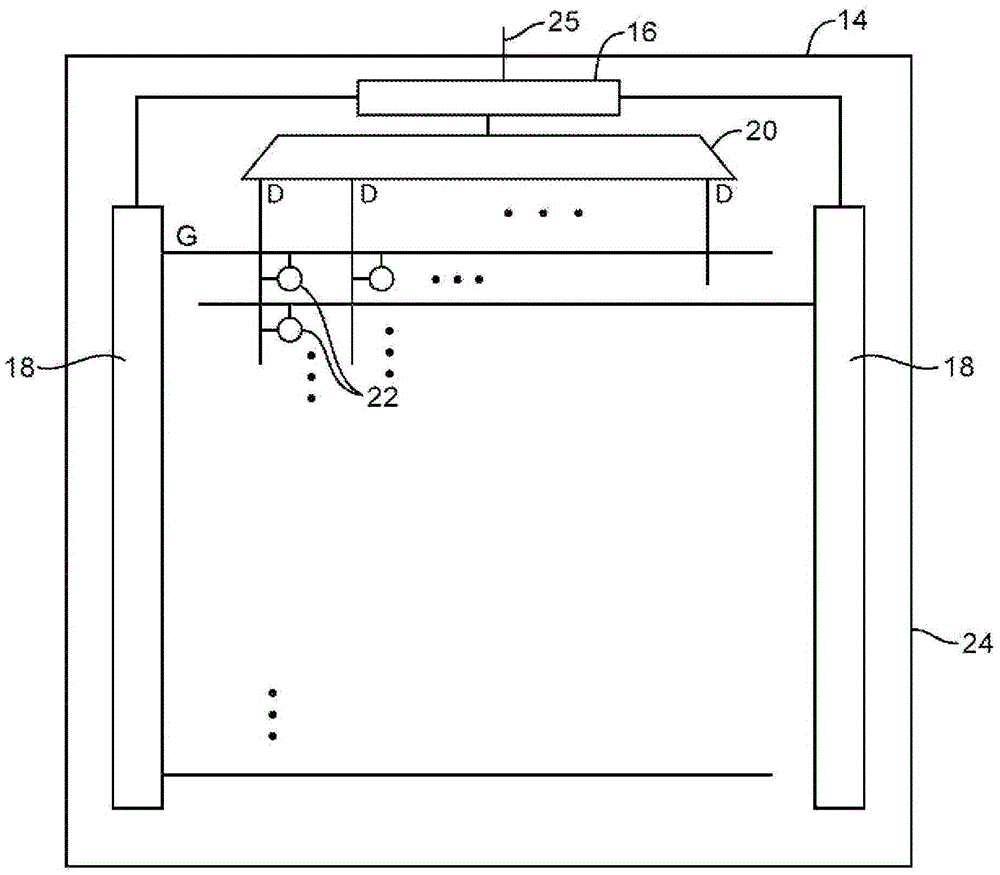
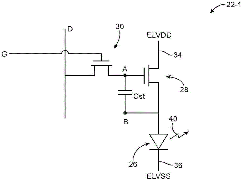
[0029] Displays in electronic devices may have driver circuits for displaying images on an array of display pixels. exist figure 1 An example display is shown in . Such as figure 1 As shown, display 14 may have one or more layers such as substrate 24 . A layer such as substrate 24 may be formed from a planar rectangular layer of material such as a planar glass layer. Display 14 may have an array of display pixels 22 for displaying images to a user. The array of display pixels 22 may be formed from rows and columns of display pixel structures on a substrate 24 . There may be any suitable number of rows and columns in the array of display pixels 22 (eg, ten or more, one hundred or more, or one thousand or more).
[0030] Solder or a conductive adhesive may be used to couple display driver circuitry such as display driver integrated circuit 16 to conductive paths such as metal traces on substrate 24 . Display driver integrated circuit 16 (sometimes referred to as a timing c...
PUM
Abstract
An electronic device may include a display having an array of display pixels on a substrate. The display pixels may be organic light-emitting diode display pixels or display pixels in a liquid crystal display. In an organic light-emitting diode display, hybrid thin-film transistor structures may be formed that include semiconducting oxide thin-film transistors, silicon thin-film transistors, and capacitor structures. The capacitor structures may overlap the semiconducting oxide thin-film transistors. Organic light-emitting diode display pixels may have combinations of oxide and silicon transistors. In a liquid crystal display, display driver circuitry may include silicon thin-film transistor circuitry and display pixels may be based on oxide thin-film transistors. A single layer or two different layers of gate metal may be used in forming silicon transistor gates and oxide transistor gates. A silicon transistor may have a gate that overlaps a floating gate structure.
Description
[0001] This patent application claims a continuation-in-part of U.S. Patent Application 14 / 249,716, filed April 10, 2014, U.S. Patent Application 14,228,098, filed March 27, 2014, U.S. Patent Application 14 / 2014, filed March 28, 2014 229,232, the priority of U.S. Patent Application 14 / 228,070, filed March 27, 2014, and Provisional Patent Application 61 / 869,937, filed August 26, 2013, which are hereby incorporated by reference in their entirety. Background technique [0002] The present invention relates generally to electronic devices, and more particularly to electronic devices having displays with thin film transistors. [0003] Electronic devices often include displays. For example, cellular telephones and portable computers include displays for presenting information to users. [0004] Displays such as liquid crystal displays are formed from multiple layers. For example, a liquid crystal display may have upper and lower polarizer layers, a color filter layer comprising a...
Claims
Application Information
Patent Timeline
Application Date:The date an application was filed.
Publication Date:The date a patent or application was officially published.
First Publication Date:The earliest publication date of a patent with the same application number.
Issue Date:Publication date of the patent grant document.
PCT Entry Date:The Entry date of PCT National Phase.
Estimated Expiry Date:The statutory expiry date of a patent right according to the Patent Law, and it is the longest term of protection that the patent right can achieve without the termination of the patent right due to other reasons(Term extension factor has been taken into account ).
Invalid Date:Actual expiry date is based on effective date or publication date of legal transaction data of invalid patent.