A preparation process of a single-layer ultra-thin substrate packaging structure with a metal shielding layer and its products

A technology of metal shielding layer and preparation process, which is applied in semiconductor/solid-state device manufacturing, electrical components, electric solid-state devices, etc., can solve the problems of short circuit between product pins and metal shielding layer, time-consuming, low production efficiency, etc., to achieve Avoid the short circuit of substrate pins, avoid repeated plating, and improve production efficiency

Active Publication Date: 2017-03-22
SUZHOU ASEN SEMICON CO LTD
View PDF4 Cites 0 Cited by
  • Summary
  • Abstract
  • Description
  • Claims
  • Application Information

AI Technical Summary

Problems solved by technology

[0003] However, for the existing single-layer ultra-thin substrate series products in the industry, if the conformal shielding process is used on this single-layer ultra-thin substrate product structure, no one has used it in the industry at present, because when the metal shielding layer is covered, it will cause The product pins form a short circuit with the metal shield
[0004] However, if the single-layer ultra-thin substrate product is to be electroplated first, the back copper needs to be removed through an etching process, and the entire product is cut into a single package structure, and then a metal shielding layer is formed on a single product. Separate operations are time-consuming and low in production efficiency

Method used


Image

  • A preparation process of a single-layer ultra-thin substrate packaging structure with a metal shielding layer and its products
  • A preparation process of a single-layer ultra-thin substrate packaging structure with a metal shielding layer and its products
  • A preparation process of a single-layer ultra-thin substrate packaging structure with a metal shielding layer and its products

Examples


Embodiment 1

[0041] A preparation process of a single-layer ultra-thin substrate packaging structure with a metal shielding layer, the preparation process steps are:

[0042] 1) Perform substrate processing to obtain a single-layer substrate:

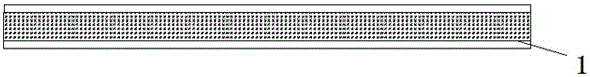
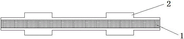
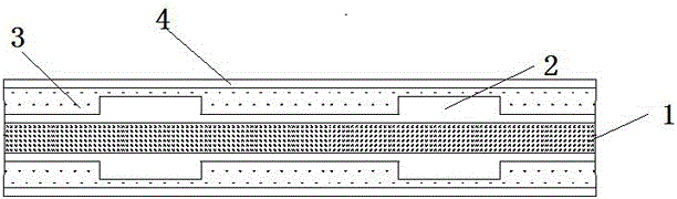
[0043] a). Take a carrier board 1, respectively press the copper layer on both sides of the carrier board 1, etch and thin the copper layer, and electroplate copper pillars 2 on the copper layer on the upper and lower surfaces of the carrier board;

[0044] b). After the electroplating of the copper pillar 2 is completed, press the BT resin layer 3 and the metal copper layer 4 on the upper and lower surfaces of the carrier plate, so that the copper pillar 2 is encapsulated in the BT resin layer 3 to obtain a matrix;

[0045] c). Open copper windows and drill holes 5 on the substrate, electroplate the opened copper windows and drill holes 5 to form pins; carry out pattern photolithography and etching on the metal copper layer 4 on the upper part of t...

Embodiment 2

[0061] On the basis of Example 1, the substrate package was carried out, and the thickness of the single-layer substrate package A1 was obtained to be 0.3 mm. When the obtained single-layer substrate package was packaged and sealed with glue, the thickness of the glue-sealing layer A2 was 0.48 mm; When half-cutting, the thickness of the reserved back copper layer A3 is 25um, the half-cut distance B between adjacent packages is 0.8mm, and the thickness C of the metal shielding layer 13 is greater than 1um; the entire single-layer ultra-thin substrate package with the metal shielding layer 13 The thickness of the structure is 0.8 mm.

[0062] A single-layer ultra-thin substrate packaging structure with a metal shielding layer prepared according to the above method, including a metal shielding layer, a glue seal, a solder mask, a nickel or gold layer, a single-layer substrate, a BT resin layer, and a packaging component , pins; the metal shielding layer is covered on the surface ...

Embodiment 3

[0064] On the basis of Example 1, after the half cut treatment, when the pins are electroless plated in step 6), a layer of nickel is first plated on the pins, and then a layer of gold is plated, which can effectively avoid The defect of short circuit when the pin is plated.

[0065] The invention designs and develops a preparation process of a single-layer ultra-thin substrate packaging structure with a metal shielding layer and its products, and realizes effective coating of the metal shielding layer of the ultra-thin packaging structure, so that the packaging structure can achieve good electromagnetic shielding and electromagnetic shielding. Compatibility, and improve the metal shielding layer coating process for products with a single-layer ultra-thin substrate package structure, using the Half cut process to coat the entire single-layer ultra-thin substrate package product with a metal shielding layer at one time, thereby improving Production efficiency; and at the pins o...


PUM


Abstract

The invention belongs to the technical field of semiconductor package, and relates to a preparation process for a single-layer ultrathin substrate package structure with a metal shielding layer and a product of the single-layer ultrathin substrate package structure. The preparation process comprises the following steps of 1) processing a substrate to obtain a single-layer substrate; 2) carrying out component package and glue sealing on the single-layer substrate to obtain a single-layer substrate package body; 3) carrying out half cut on the single-layer substrate package body by a half cut process to form independent package bodies connected by back copper; 4) carrying out metal shielding layer electroplating on the surface outside of the back copper of the independent package bodies connected by the back copper; 5) removing the back copper at a connection part of a bottom layer, exposing a pin at the bottom surface to obtain an independent half-finished package body; and 6) carrying out concentrated overturning and fixing on the half-finished package body, and carrying out concentrated processing on the pin at the bottom surface. According to the preparation process, the half cut process is used for separating chemical plating processing of the pin from electroplating processing of the metal shielding layer, so that repeated electroplating of the pin is avoided, concentrated and unified processing can be carried out on the metal shielding layer and the pin of the single-layer ultrathin substrate package structure, and the production efficiency is improved.

Description

technical field [0001] The invention belongs to the technical field of semiconductor packaging, and in particular relates to a preparation process of a single-layer ultra-thin substrate packaging structure with a metal shielding layer and a product thereof. Background technique [0002] Electromagnetic Compatibility EMC (Electro-Magnetic Compatibility) is the ability of the electromagnetic energy generated by the equipment to neither interfere with other equipment nor be disturbed by the electromagnetic energy of other equipment. If the circuit modules in a circuit system can work harmoniously and normally without causing electromagnetic interference to cause performance changes or failure to work, the circuit system is said to be compatible with each other. However, with the rapid development of electronic technology, the circuit functions are becoming more and more diversified, the structure is becoming more and more complicated, the working power is gradually increasing, ...

Claims


Application Information

Patent Timeline
Patent Type & Authority Patents(China)
IPC IPC(8): H01L23/28H01L23/13H01L21/56
CPCH01L21/56H01L23/13H01L23/28H01L2224/16245H01L2224/18H01L2224/97H01L2924/15311H01L2924/3025H01L2224/81H01L2224/85
Inventor 郭桂冠王政尧
Owner SUZHOU ASEN SEMICON CO LTD
Why Eureka
Try Eureka