Multi-active zone epitaxial structure, semiconductor laser adopting same and manufacturing method of multi-active zone epitaxial structure

A technology of epitaxial structure and manufacturing method, which is applied in the direction of semiconductor lasers, lasers, laser components, etc., can solve the problems of increasing the far-field divergence angle of semiconductor lasers and deteriorating beam quality, so as to increase the burden of heat dissipation, reduce the diffraction effect, Effect of Reducing Power Density

Inactive Publication Date: 2016-03-23
INST OF SEMICONDUCTORS - CHINESE ACAD OF SCI +1
View PDF7 Cites 15 Cited by
  • Summary
  • Abstract
  • Description
  • Claims
  • Application Information

AI Technical Summary

Problems solved by technology

In addition, high power output means that a large thickness of the waveguide layer is required, and lasing of high-order transverse modes

Method used


Image

  • Multi-active zone epitaxial structure, semiconductor laser adopting same and manufacturing method of multi-active zone epitaxial structure
  • Multi-active zone epitaxial structure, semiconductor laser adopting same and manufacturing method of multi-active zone epitaxial structure
  • Multi-active zone epitaxial structure, semiconductor laser adopting same and manufacturing method of multi-active zone epitaxial structure

Examples


Embodiment Construction

[0030] In order to make the object, technical solution and advantages of the present invention clearer, the present invention will be further described in detail below in conjunction with specific embodiments and with reference to the accompanying drawings.

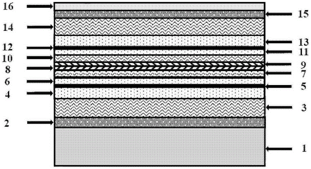
[0031] The invention discloses a tunnel cascade epitaxial structure with multiple active regions, comprising:

[0032] a substrate;

[0033] A plurality of active regions, the plurality of active regions are sequentially formed on the substrate, and the plurality of active regions are connected through a reverse-biased PN junction.

[0034] Wherein, in the reverse biased PN junction, the thickness of the P-type material is 10-20 nm, and the thickness of the N-type material is 10-20 nm.

[0035] Preferably, the reverse-biased PN junction is composed of a stacked P-type GaAs layer and an N-type GaAs layer.

[0036] Preferably, each of the plurality of active regions includes a lower confinement layer, a lower waveguide la...


PUM

PropertyMeasurementUnit
Thicknessaaaaaaaaaa

Abstract

The invention relates to a tunnel cascaded multi-active region epitaxial structure. The tunnel cascaded multi-active region epitaxial structure includes a substrate and a plurality of heterostructure active regions which are limited respectively; the plurality of active regions are formed on the substrate sequentially; and the plurality of active regions are connected with each other through reversely-biased PN junctions. The invention also provides a semiconductor laser adopting the epitaxial structure. According to the laser, a buffer layer and an electrode contact layer are sequentially grown on the uppermost active region; and follow-up laser fabrication is completed through using a standard wide-surfaced strip-shaped laser fabrication process. The number of active regions in the epitaxial structure can be adjusted between 2 to 4 according to needs. With the tunnel cascaded multi-active region epitaxial structure and the laser adopting the same adopted, output power and slope efficiency can be improved, and a vertical divergence angle can be greatly reduced.

Description

technical field [0001] The invention relates to the technical field of high-power semiconductor lasers, in particular to a multi-active region epitaxial structure, a semiconductor laser using the same and a manufacturing method thereof. Background technique [0002] In recent years, semiconductor lasers have been widely used in military, industrial processing, precision measurement, laser medical treatment, optical Communication, optical storage and laser printing have been widely and far-reaching applications. Due to its high output power, high-power semiconductor lasers have developed rapidly in industrial fields such as metal cutting, laser cladding, and deep penetration welding, as well as aerospace, national defense and military applications. [0003] The main factor limiting the further improvement of the output power of near-infrared high-power semiconductor lasers is the optical catastrophic damage of the cavity surface. Therefore, optimizing the epitaxial structur...

Claims


Application Information

Patent Timeline
IPC IPC(8): H01S5/343
CPCH01S5/3432
Inventor 侯继达熊聪刘素平马骁宇
Owner INST OF SEMICONDUCTORS - CHINESE ACAD OF SCI
Why Eureka
Try Eureka