Compound, organic electroluminescence element material, ink composition, organic electroluminescence element, electronic device, and method for producing compound

一种化合物、键合的技术,应用在化合物领域,能够解决多种要求特性不充分等问题,达到高效简便制造的效果

Inactive Publication Date: 2016-03-23
IDEMITSU KOSAN CO LTD
View PDF17 Cites 2 Cited by
  • Summary
  • Abstract
  • Description
  • Claims
  • Application Information

AI Technical Summary

Problems solved by technology

Therefore, the properties of the compounds verified in Patent Document 10 are limited to the range of combining multiple biscarbazole-containing groups with the same structure and unfused nitrogen-containing rings, and it is not sufficient to satisfy various required properties of organic EL devices.

Method used


Image

  • Compound, organic electroluminescence element material, ink composition, organic electroluminescence element, electronic device, and method for producing compound
  • Compound, organic electroluminescence element material, ink composition, organic electroluminescence element, electronic device, and method for producing compound
  • Compound, organic electroluminescence element material, ink composition, organic electroluminescence element, electronic device, and method for producing compound

Examples


Embodiment 1

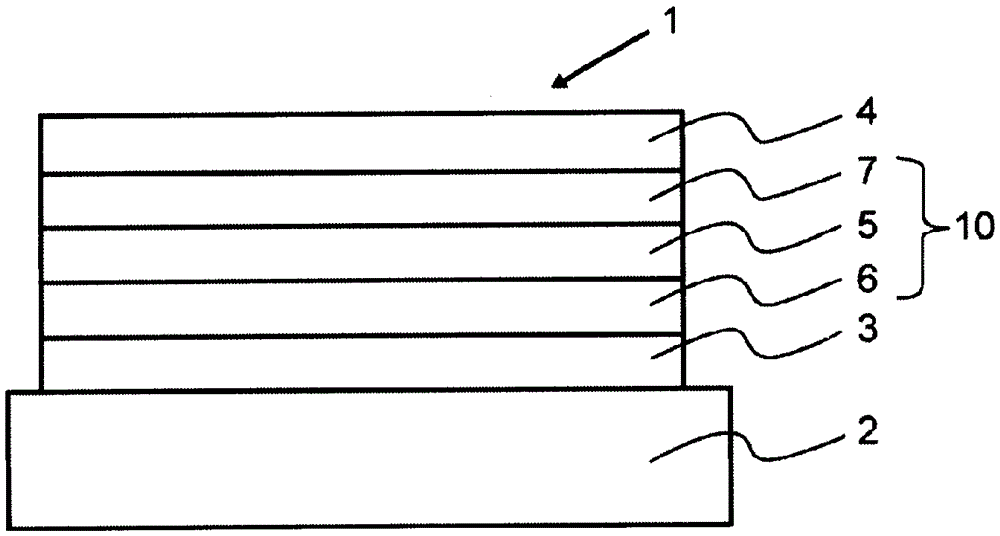
[1120] (Substrate washing)

[1121] A 25 mm x 25 mm x 1.1 mm thick glass substrate with an ITO transparent electrode (manufactured by Geomatec Co., Ltd.) was ultrasonically cleaned in isopropanol for 5 minutes, and then UV ozone was washed for 5 minutes.

[1122] (formation of basal layer)

[1123] On the above-mentioned ITO substrate, CLEVIOUS AI4083 (trade name) manufactured by HERAEUS Co., Ltd. as a hole transport material was formed into a film with a thickness of 30 nm by the spin coating method. After the film formation, unnecessary parts were removed with acetone, and then fired on a hot plate at 200° C. for 10 minutes in the air to produce a base substrate.

[1124] (Formation of luminescent layer)

[1125] Compound H-4 obtained in Synthesis Example 4 was used as a host material, and the following compound D-1 was used as a dopant material, and mixed so that the mass ratio of compound H-4: compound D-1 was 90:10 A mixing ratio of 1.6 mass % was prepared in toluene. ...

Embodiment 2

[1130] An organic EL device was produced in the same manner as in Example 1 except that Compound D-2 was used as a dopant material. The measurement results are shown in Table 1.

Embodiment 3

[1136] Using the compound H-13 obtained in Synthesis Example 13 as the host material and the following compound D-1 as the dopant material, the mixing ratio of compound H-13:compound D-1 reached 95:5 in terms of weight ratio An organic EL element was fabricated by the same method as in Example 1 except that a 1.6% by weight toluene solution was prepared. The measurement results are shown in Table 1.


PUM

PropertyMeasurementUnit
strengthaaaaaaaaaa
Weight-average Molecular Weightaaaaaaaaaa
molecular weightaaaaaaaaaa

Abstract

Provided are a compound represented by formula (1) (in the formula, *a, *b, R1, X1, L1, L2, n, A1, and A2 are as defined in the specification) and a method for producing a compound represented by formula (1) that introduces A1 under reaction conditions that make the reaction activity of Hal2 of a compound represented by formula (I) (in the formula, *c, *d, R1, X1, L1, L2, n, A1, A2, Hal1, and Hal2 are as defined in the specification) markedly lower than that of Hal1, then introduces A2 different from A1 under reaction conditions that raise the reaction activity of Hal2. A compound represented by formula (1) can form a layer by coating and can respond to the diverse property requirements of an EL element.

Description

technical field [0001] The present invention relates to a compound, a material for an organic electroluminescent element, an organic electroluminescent element, an ink composition, an electronic device, and a method for producing the aforementioned compound. Background technique [0002] An organic electroluminescent element (hereinafter, sometimes referred to as "organic EL element") is known, which has an organic thin film layer including a light emitting layer between an anode and a cathode, and is formed by injecting Light is emitted from the energy of excitons generated by the recombination of holes and electrons in the light-emitting layer. [0003] Organic EL elements are expected as light-emitting elements with high luminous efficiency, high image quality, low power consumption, and thin design, taking advantage of their advantages as self-luminous elements. It is known to form a light-emitting layer as a host / dopant light-emitting layer in which a host is doped wit...

Claims


Application Information

Patent Timeline
Patent Type & Authority Applications(China)
IPC IPC(8): C07D403/14C09D11/037C09D11/50C09K11/06H01L51/50
CPCC07D403/14C09K11/06C09K2211/1011C09K2211/1029C09K2211/1033C09K2211/1037C09K2211/1044C09K2211/1059C09K2211/1088C09K2211/1092C09K2211/185C09D11/037C09D11/50C09D11/52C09K11/025C09K2211/1007C09B57/00C09B69/109C09B57/008H10K85/636H10K85/633H10K85/654H10K85/6572H10K85/342H10K50/11H10K2101/10H10K85/615H10K50/15H10K30/865H10K50/16
Inventor 池田洁川上宏典
Owner IDEMITSU KOSAN CO LTD
Why Eureka
Try Eureka