Liquid crystal display device and driving method thereof
A technology of a liquid crystal display device and a driving method, which is applied to static indicators, instruments, etc., can solve the problems of affecting the display quality of the display device, abnormal screen display, insufficient charging of pixel units, etc., so as to avoid abnormal screen display, improve stability, The effect of improving the display quality
- Summary
- Abstract
- Description
- Claims
- Application Information
AI Technical Summary
Problems solved by technology
Method used
Image
Examples
no. 1 example
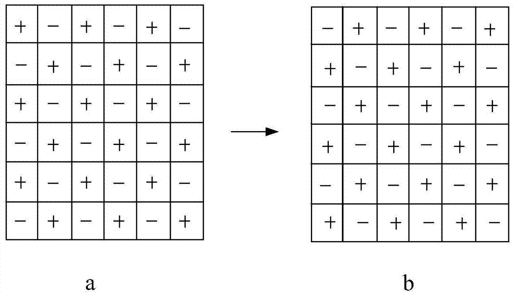
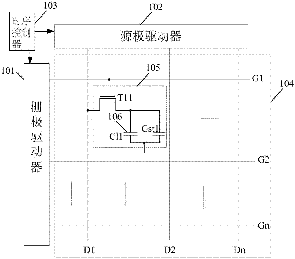
[0030] image 3 It is a schematic structural diagram of a liquid crystal display device provided by the first embodiment of the present invention. Figure 4 Yes image 3 The shown schematic diagram of the polarity conversion of the pixel unit of the liquid crystal display device. Please refer to image 3 with Figure 4 The liquid crystal display device includes a gate driver 101, a source driver 102, a timing controller 103, and a display panel 104.
[0031] Wherein, the display panel 104 is provided with a plurality of gate lines G1-Gn connected with the gate driving circuit 101, a plurality of data lines D1-Dn connected with the source driver 102, and the gate lines and the data lines are defined Each pixel unit 105 includes a thin film transistor T11, a liquid crystal capacitor Cl1 and a storage capacitor Cst1. The gate of the thin film transistor T11 is connected to the corresponding gate line, the source is connected to the corresponding data line, and the drain The electrod...
no. 2 example
[0044] Image 6 It is a flow chart of the steps of the driving method of the liquid crystal display device provided by the second embodiment of the present invention. Please refer to Figure 3 to Figure 6 The driving method of the liquid crystal display device of this embodiment may include the following steps: steps 601-605.
[0045] Step 601: The timing controller outputs a first control signal to the gate driver, and outputs a second control signal to the source driver.
[0046] Step 603: The gate driver sequentially outputs gate driving signals to each gate line according to the first control signal, so as to turn on the thin film transistors connected to each gate line.
[0047] Step 605: When the gate driver outputs the gate driving signal to each gate line, the source driver outputs a data driving signal to each data line according to the second control signal, so that each data line is loaded with data driving Signal; wherein, the source driver controls the positive and neg...
PUM
 Abstract
Description
Claims
Application Information


