
Resistive random access memory circuit and reading method

A resistive random access memory technology, applied in static memory, digital memory information, information storage, etc., can solve problems such as read interference

Active Publication Date: 2017-12-01
WINBOND ELECTRONICS CORP
View PDF4 Cites 0 Cited by
  • Summary
  • Abstract
  • Description
  • Claims
  • Application Information

AI Technical Summary

Problems solved by technology

[0004] The purpose of the present invention is to provide a resistive random access memory circuit to solve the technical problem of read disturbance when the bit line voltage level is too high

Method used


Image

  • Resistive random access memory circuit and reading method
  • Resistive random access memory circuit and reading method
  • Resistive random access memory circuit and reading method

Examples


Embodiment Construction

[0061] Preferred embodiments according to the present invention will be described below. It must be noted that the present invention provides many applicable inventive concepts, and the specific embodiments disclosed here are only used to illustrate specific ways to achieve and use the present invention, and are not intended to limit the scope of the present invention.

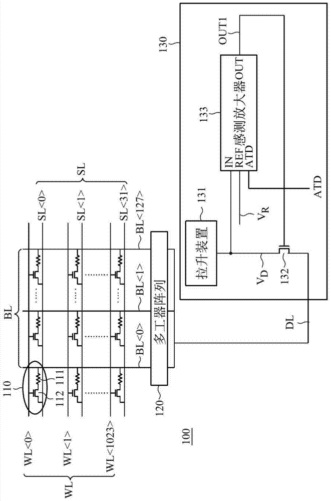
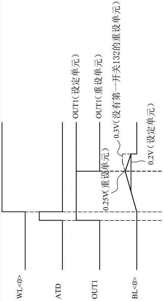
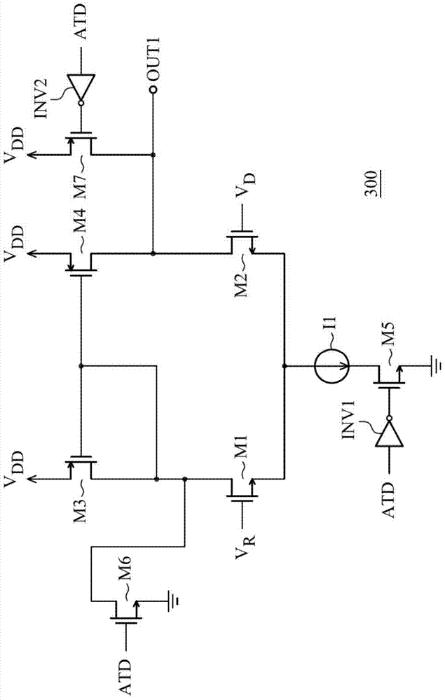
[0062] figure 1 A schematic diagram of a resistive random access memory circuit according to an embodiment of the invention is shown. Such as figure 1 As shown, a resistive random access memory (resistance random access memory, RRAM) circuit 100 includes a word line array WL, a source line array SL, a bit line array BL, a plurality of memory cells (including the memory cell 110), a multiplexer Array 120 and sensing module 130 . The word line array WL includes an array of multiple word lines parallel to each other, the source line array SL includes an array of multiple source lines parallel to each other, an...


PUM


Abstract

The invention provides a resistance random access memory circuit and a reading method thereof. The circuit comprises word lines, bit lines, source lines, memory cells and a sensing module group. Each of the memory cells comprises a resistor and a transistor. The resistor is switched between high impedance and low impedance, and a node is coupled with one of the bit lines. The transistor is controlled by one of the word lines, and is coupled between the resistor and one of the source lines. The sensing module group comprises a switch and a sense amplifier. The switch is controlled by output signals, and is coupled with one of the bit lines. The sense amplifier compares a data voltage generated by current which flows through the switch and the resistor with a reference voltage in order to generate an output signal; if the data voltage exceeds the reference voltage, the switch is not conducted; if the data voltage is lower than the reference voltage, the switch is conducted. The selected memory cell is coupled with a ground terminal and begins to discharge, so that read disturbance is reduced and even eliminated.

Description

technical field [0001] The present invention relates to a circuit and a reading method of a resistive random access memory, in particular to a circuit and a reading method for reducing the voltage level of read disturbance on a bit line. Background technique [0002] Recently, new non-volatile memory devices, such as resistance random access memory (RRAM), have been proposed. A cell of RRAM includes a voltage storage element having two electrodes and a layer of variable resistive material between the two electrodes. The variable resistance material layer, that is, the data storage material layer, can make the resistive material layer form a filament, a conductive path or a low resistance path according to the application of an electrical signal (voltage or current) between the electrodes, And it has a reversible change in the resistance value. [0003] However, the current RRAM has the concern of read disturbance. If the bit line voltage level is higher than a specific vo...

Claims


Application Information

Patent Timeline
Patent Type & Authority Patents(China)
IPC IPC(8): G11C13/00
Inventor 柳德铉
Owner WINBOND ELECTRONICS CORP
Learn More