vertically magnetized mtj device
A vertical magnetization and device technology, applied in the direction of magnetic field controlled resistors, etc., can solve the problems of reduced erasable times, MTJ breakdown, increased power consumption, etc., to reduce the write current, increase the effective thickness, and reduce the size Effect
- Summary
- Abstract
- Description
- Claims
- Application Information
AI Technical Summary
Problems solved by technology
Method used
Image
Examples
example 1
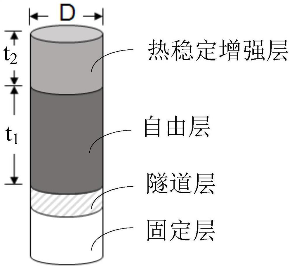
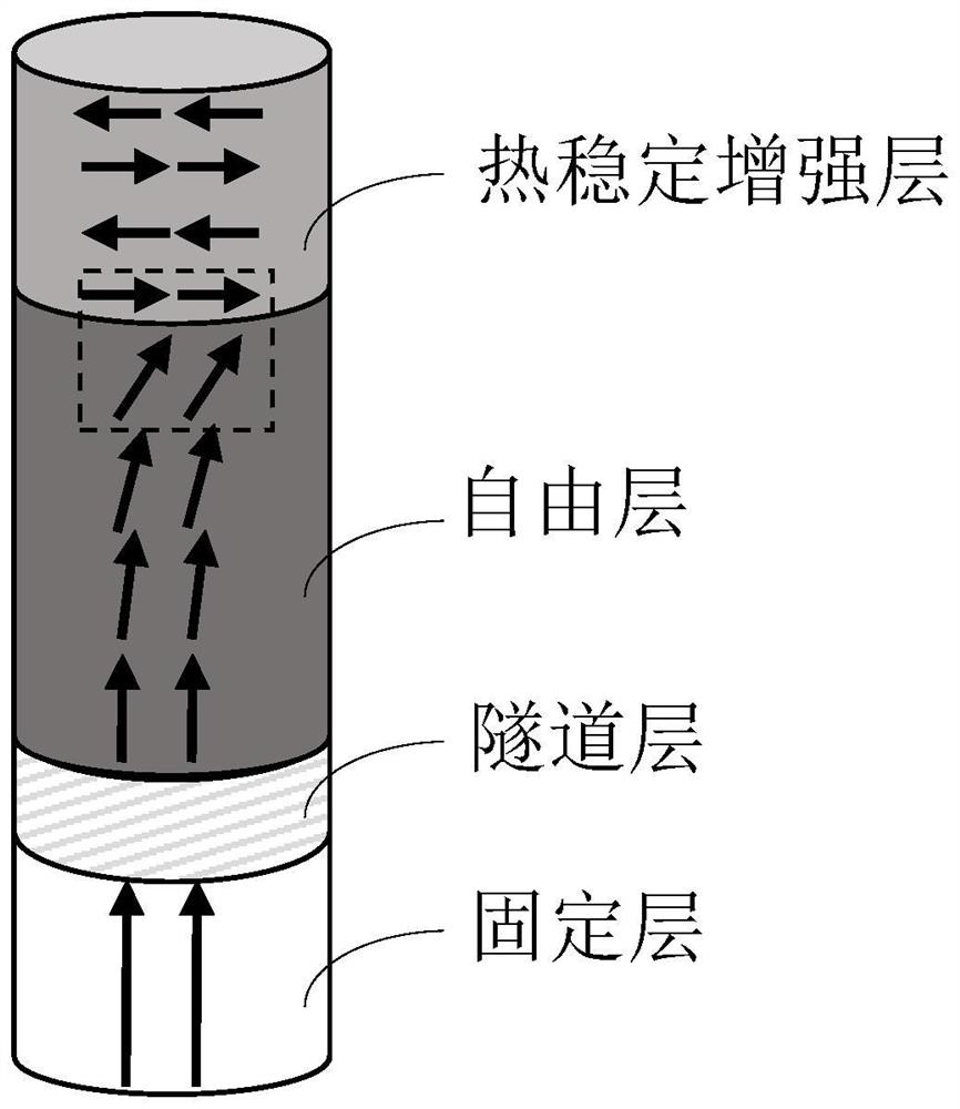
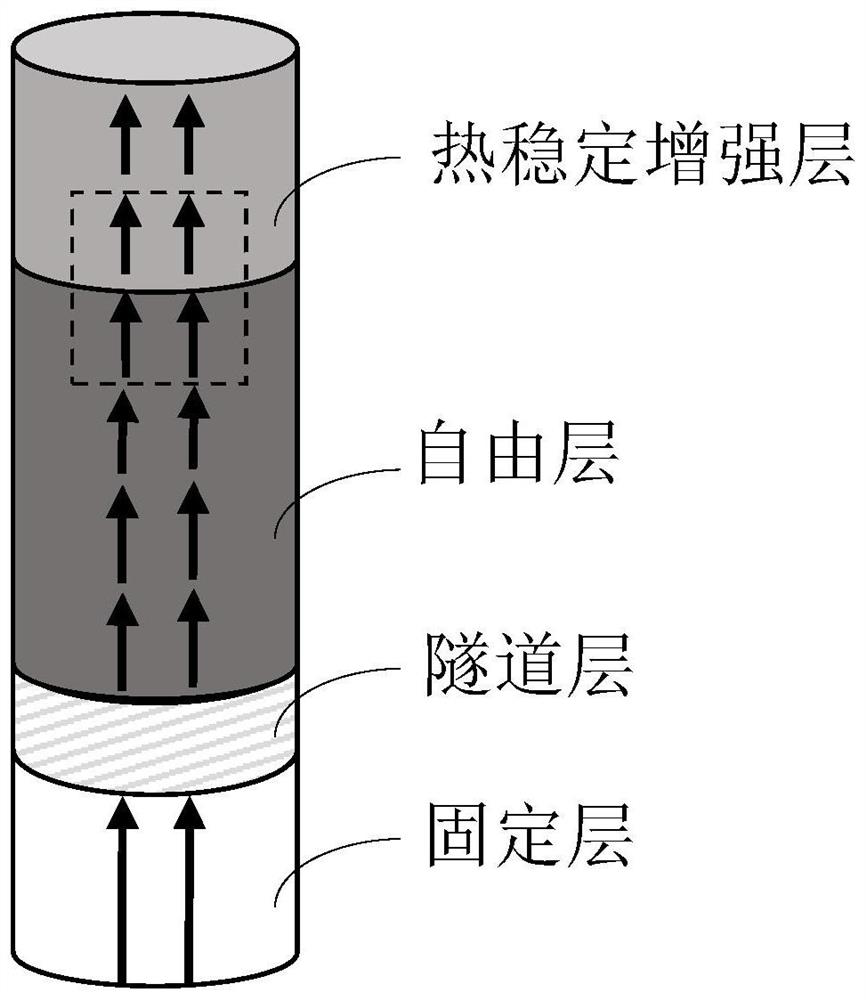
[0041] The MTJ device with vertical magnetization, from top to bottom, is a thermally stable enhancement layer, a free layer, a tunnel layer and a fixed layer. The diameter D of the MTJ device is 10nm, and the material of the thermally stable enhancement layer is Fe 0.5 Rh 0.5 , Fe atoms and Rh atoms each account for 50% of the total number of atoms, and its thickness is 9nm; the material of the free layer is FeB, and its thickness is 14nm; the material of the tunnel layer is HfO 2 , and its thickness is 0.6nm; the pinned layer includes a reference magnetic layer and a synthetic antiferromagnetic pinning layer, wherein the material of the reference magnetic layer is CoFe, and its thickness is 2nm, and the structure of the synthetic antiferromagnetic pinning layer is [Pd( 0.6) / Co(0.4)] 8 / Ir(0.4) / [Co(0.4) / Pd(0.6)] 4 Multi-layer film structure, the value in parentheses indicates the corresponding film thickness, the unit is nm, the value outside the brackets, such as 8,4, indi...
example 2
[0043] The MTJ device with vertical magnetization, from top to bottom, is a thermally stable enhancement layer, a free layer, a tunnel layer and a fixed layer. The diameter D of the MTJ device is 12nm, and the material of the thermally stable enhancement layer is Fe 0.5 Rh 0.45 Pt 0.05 , Fe atoms account for 50% of the total number of atoms, Rh atoms account for 45% of the total number of atoms, Pt atoms account for 5% of the total number of atoms, and its thickness is 10nm; the material of the free layer is CoFeB, and its thickness is 16nm; the material of the tunnel layer is MgO with a thickness of 0.8nm; the pinned layer includes a reference magnetic layer and a synthetic antiferromagnetic pinning layer, wherein the material of the reference magnetic layer is CoFeB with a thickness of 2nm, and the structure of the synthetic antiferromagnetic pinning layer is [Pt (0.4) / Co(0.4)] 4 / Ru(0.4) / [Co(0.4) / Pt(0.4)] 2 Multi-layer film structure, the value in parentheses indicates t...
PUM
| Property | Measurement | Unit |
|---|---|---|
| phase transition temperature | aaaaa | aaaaa |
| thickness | aaaaa | aaaaa |
| thickness | aaaaa | aaaaa |
Abstract
Description
Claims
Application Information


