Atomic layer etching device and atomic layer etching method using same

An atomic layer etching and production device technology, which is applied in the manufacture of discharge tubes, electrical components, semiconductor/solid-state devices, etc. The effect of increasing the etching rate and saving the amount of use

Active Publication Date: 2016-03-30
BEIJING NAURA MICROELECTRONICS EQUIP CO LTD
View PDF5 Cites 10 Cited by
  • Summary
  • Abstract
  • Description
  • Claims
  • Application Information

AI Technical Summary

Problems solved by technology

The atomic layer etching technology in the related art has disadvantages such as long etching period, low etching efficiency, and complicated equipment.

Method used


Image

  • Atomic layer etching device and atomic layer etching method using same
  • Atomic layer etching device and atomic layer etching method using same
  • Atomic layer etching device and atomic layer etching method using same

Examples


Embodiment Construction

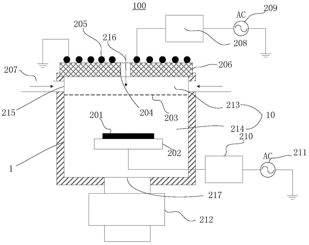
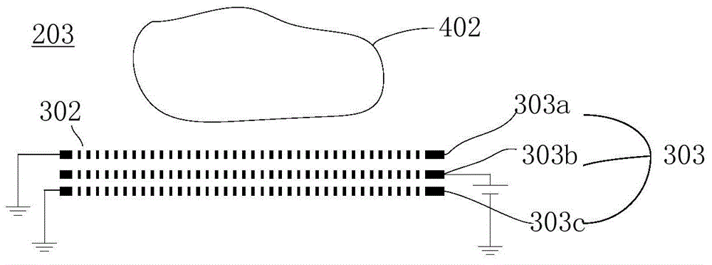
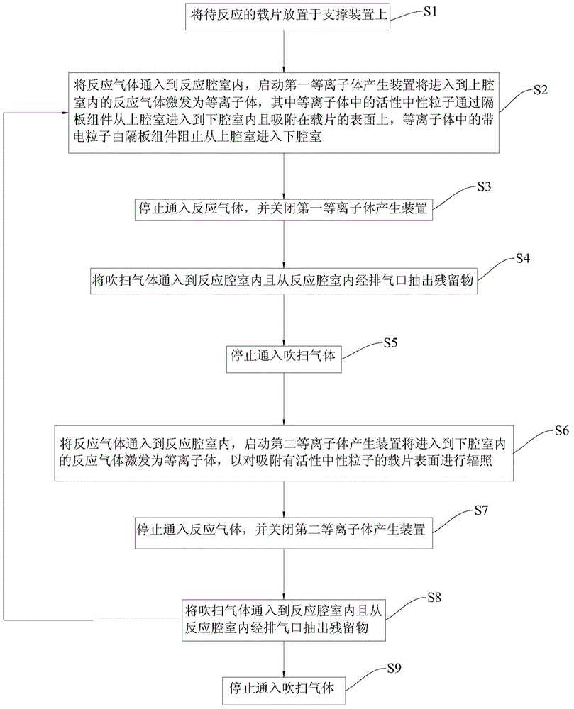
[0038] The embodiments of the present invention are described in detail below. Examples of the embodiments are shown in the accompanying drawings, in which the same or similar reference numerals indicate the same or similar elements or elements with the same or similar functions. The embodiments described below with reference to the accompanying drawings are exemplary, and are intended to explain the present invention, but should not be construed as limiting the present invention.

[0039] In the description of the present invention, it should be understood that the terms "center", "longitudinal", "transverse", "length", "width", "thickness", "upper", "lower", "front", " "Back", "Left", "Right", "Vertical", "Horizontal", "Top", "Bottom", "Inner", "Outer", "Axial", "Radial", "Circumferential", etc. The indicated orientation or positional relationship is based on the orientation or positional relationship shown in the drawings, and is only for the convenience of describing the pres...


PUM


Abstract

The invention discloses an atomic layer etching device and an atomic layer etching method using the same. The atomic layer etching device comprises a reaction chamber, a separator assembly, a first plasma generating device and a second plasma generating device. The separator assembly divides the reaction chamber into an upper chamber and a lower chamber. The separator assembly comprises separators that can be grounded or connected to a DC bias power supply to stop charged particles in the upper chamber from entering the lower chamber and allow active and neutral particles to enter the lower chamber. The first plasma generating device is used for exciting gas entering the upper chamber into plasmas. The second plasma generating device is used for exciting gas entering the lower chamber into plasmas. By using active adsorption particle chemical adsorption instead of traditional reaction gas adsorption, the atomic layer etching device can significantly improve the etching rate, shorten the etching cycle length, save the amount of etching reaction gas, and reduce the process cost.

Description

Technical field [0001] The invention relates to the field of etching, in particular to an atomic layer etching device and an atomic layer etching method using the same. Background technique [0002] At present, atomic layer deposition (Atomic Layer Deposition, ALD) has been widely used in the semiconductor industry and is a mainstream process for preparing high-K gate dielectric layers of field effect transistors. Corresponding to the subtraction process, atomic layer etching (Atomic Layer Etching, ALE) has also been developed along with the needs of the application. The first alternative of Cl2 adsorption and electron beam etching was used to achieve GaAs atomic layer etching. The atomic layer etching technology in the related art has disadvantages such as long etching period, low etching efficiency, and complicated equipment. Summary of the invention [0003] The present invention aims to solve one of the technical problems in the related art at least to a certain extent. To t...

Claims


Application Information

Patent Timeline
Patent Type & Authority Applications(China)
IPC IPC(8): H01J37/32
CPCH01L21/00
Inventor 罗巍
Owner BEIJING NAURA MICROELECTRONICS EQUIP CO LTD
Why Eureka
Try Eureka