Method and apparatus for uniformly reducing the characteristic wet etch rate of a silicon nitride film

A wet etching, rate technology, applied in gaseous chemical plating, coating, discharge tube, etc., can solve the problem of difficult to achieve SiN film

Active Publication Date: 2018-10-19
LAM RES CORP
View PDF15 Cites 0 Cited by
  • Summary
  • Abstract
  • Description
  • Claims
  • Application Information

AI Technical Summary

Problems solved by technology

However, forming such etch-resistant SiN films via ALD processes is difficult to achieve within typical thermal budget constraints.

Method used


Image

  • Method and apparatus for uniformly reducing the characteristic wet etch rate of a silicon nitride film
  • Method and apparatus for uniformly reducing the characteristic wet etch rate of a silicon nitride film
  • Method and apparatus for uniformly reducing the characteristic wet etch rate of a silicon nitride film

Examples


Embodiment

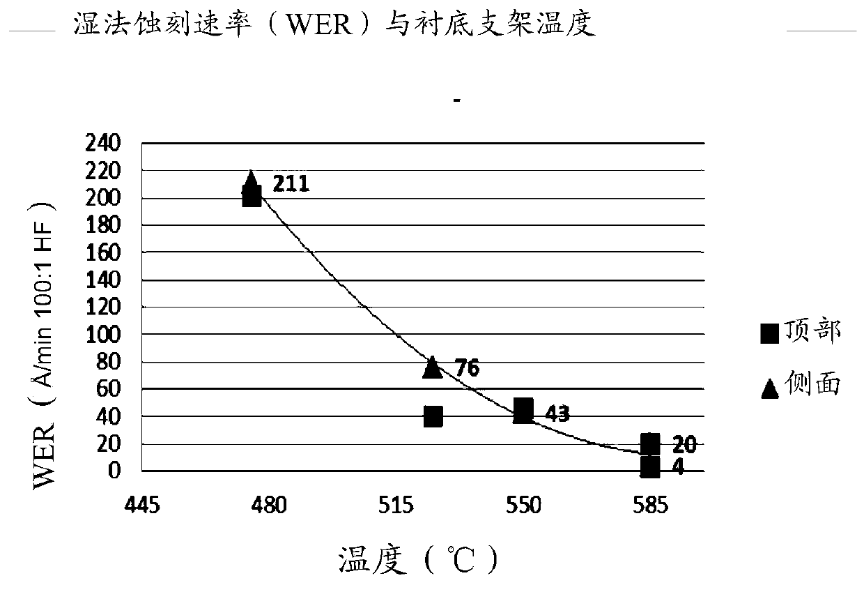
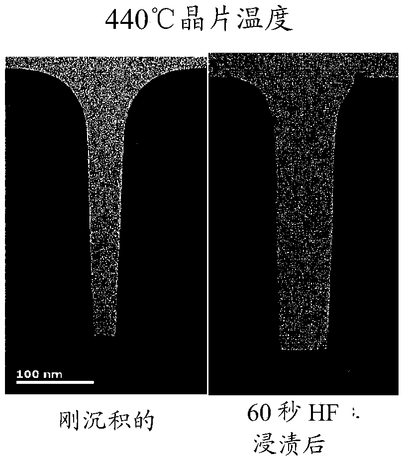
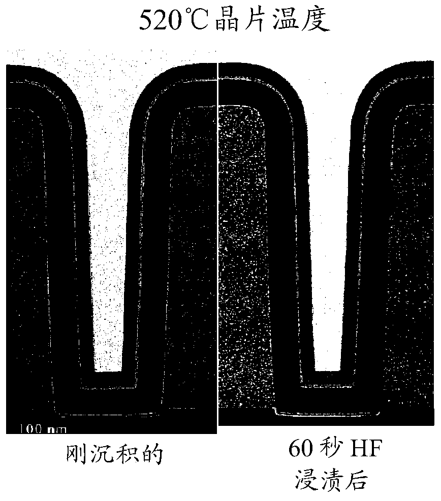
[0052] Figure 4A and 4B Results are shown for a first set of example SiN films deposited using various ALD-type film formation techniques. in particular, Figure 4A The wet etch rates (WER ). The WER was determined by measuring the amount of SiN film etched away on each area (top and sidewall) after exposure to a 100:1 molar ratio HF solution at 23 °C and 760 Torr. The solution was not stirred nor the substrate was shaken during the exposure (ie, the HF solution was substantially stationary / immobile relative to the substrate). (Some stirring mechanisms apparently tend to slightly increase WER). The amount of etched SiN film was determined by transmission electron microscopy (TEM), Figure 4B TEM images of the as-deposited and etched high-aspect features for processes (1 ), and (3)-(7) are shown.

[0053] exist Figure 4A Starting at the far left in , process (1) is the benchmark ALD process that results in the deposition of a SiN film with a very high WER on both the ...


PUM


Abstract

Disclosed herein are methods and apparatus directed to uniformly reducing intra-feature wet etch rates of silicon nitride films, and in particular to methods for depositing SiN films with reduced wet etch rates. The method may include adsorbing a Si-containing film precursor onto a semiconductor substrate in a processing chamber to form an adsorption-limited layer of the precursor, and then removing the unadsorbed precursor from the volume surrounding the adsorbed precursor . The adsorbed precursor can then be reacted by exposing it to a plasma containing N-containing ions and / or groups to form a SiN film layer on the substrate, which can then be reacted by exposing the SiN film layer to He plasma. The SiN film layer is dense. The aforementioned steps can then be repeated to form another dense SiN film layer on the substrate. Also disclosed herein are apparatuses employing the aforementioned techniques for depositing SiN films with reduced wet etch rates on semiconductor substrates.

Description

technical field [0001] The present invention relates generally to the field of semiconductor processing, and more particularly to methods and apparatus for uniformly reducing wet etch rates within features of silicon nitride films. Background technique [0002] In the semiconductor industry, as device and feature sizes continue to shrink, and as three-dimensional device structures (for example, Intel Corporation's tri-gate transistor architecture) become more common in integrated circuit (IC) design, depositing thin The ability of conformal films (films of material with a uniform thickness corresponding to the shape of the underlying structure, even though the underlying structure is not flat) will continue to be appreciated. Atomic layer deposition (ALD) is a film formation technique well suited for depositing conformal films due to the fact that a single cycle of ALD deposits only a single thin layer of material, the thickness of which is limited by the chemical reactions ...

Claims


Application Information

Patent Timeline
Patent Type & Authority Patents(China)
IPC IPC(8): H01L21/31H01L21/02H01L21/67H01J37/32
CPCH01J37/32H01L21/02208H01L21/02252H01L21/31H01L21/67011C23C16/345C23C16/56H01L21/0217H01L21/0228H01L21/0234C23C16/45536C23C16/52
Inventor 詹姆斯·S·思姆斯凯瑟琳·M·凯尔克纳乔恩·亨利丹尼斯·M·豪斯曼
Owner LAM RES CORP
Why Eureka
Try Eureka