
Method for decreasing wet etching speed of silicon nitride

A wet etching, silicon nitride technology, applied in electrical components, semiconductor/solid-state device manufacturing, circuits, etc., can solve the problems of fast wet etching rate, increase the contact resistance of the connection diffusion area, reduce the thermal budget, etc., to improve the etching selection. rate, the effect of reducing the wet etch rate

Inactive Publication Date: 2005-02-02
WINBOND ELECTRONICS CORP
View PDF1 Cites 0 Cited by
  • Summary
  • Abstract
  • Description
  • Claims
  • Application Information

AI Technical Summary

Problems solved by technology

Although the LPCVD silicon nitride layer deposited at 700-800°C in the traditional way can be used as an etch stop layer, in the manufacturing process of stacked DRAM, since the capacitor is made after the transistor is formed, if the LPCVD deposited at high temperature is used The silicon nitride layer will increase the contact resistance of the connecting diffusion region, which will affect the performance of the transistor
Therefore, if the LPCVD silicon nitride layer deposited at low temperature can be used here, it will help reduce the thermal budget, but first, the problem of its wet etching rate being too fast must be solved

Method used


Image

  • Method for decreasing wet etching speed of silicon nitride
  • Method for decreasing wet etching speed of silicon nitride
  • Method for decreasing wet etching speed of silicon nitride

Examples


Embodiment Construction

[0051] In order to make the above and other objects, features, and advantages of the present invention more comprehensible, the preferred embodiments are specifically listed below, together with the accompanying drawings, and are described in detail as follows:

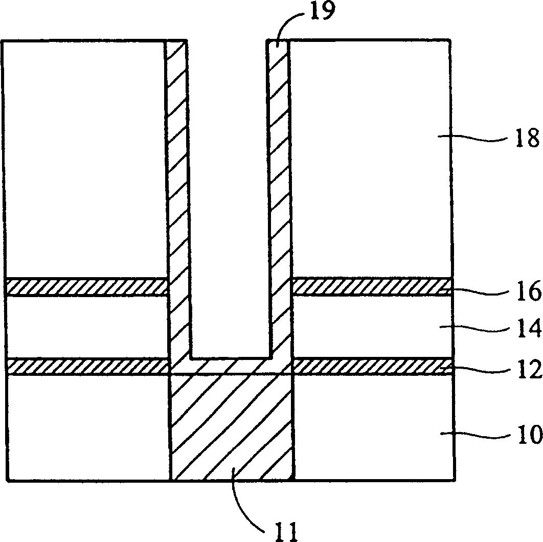
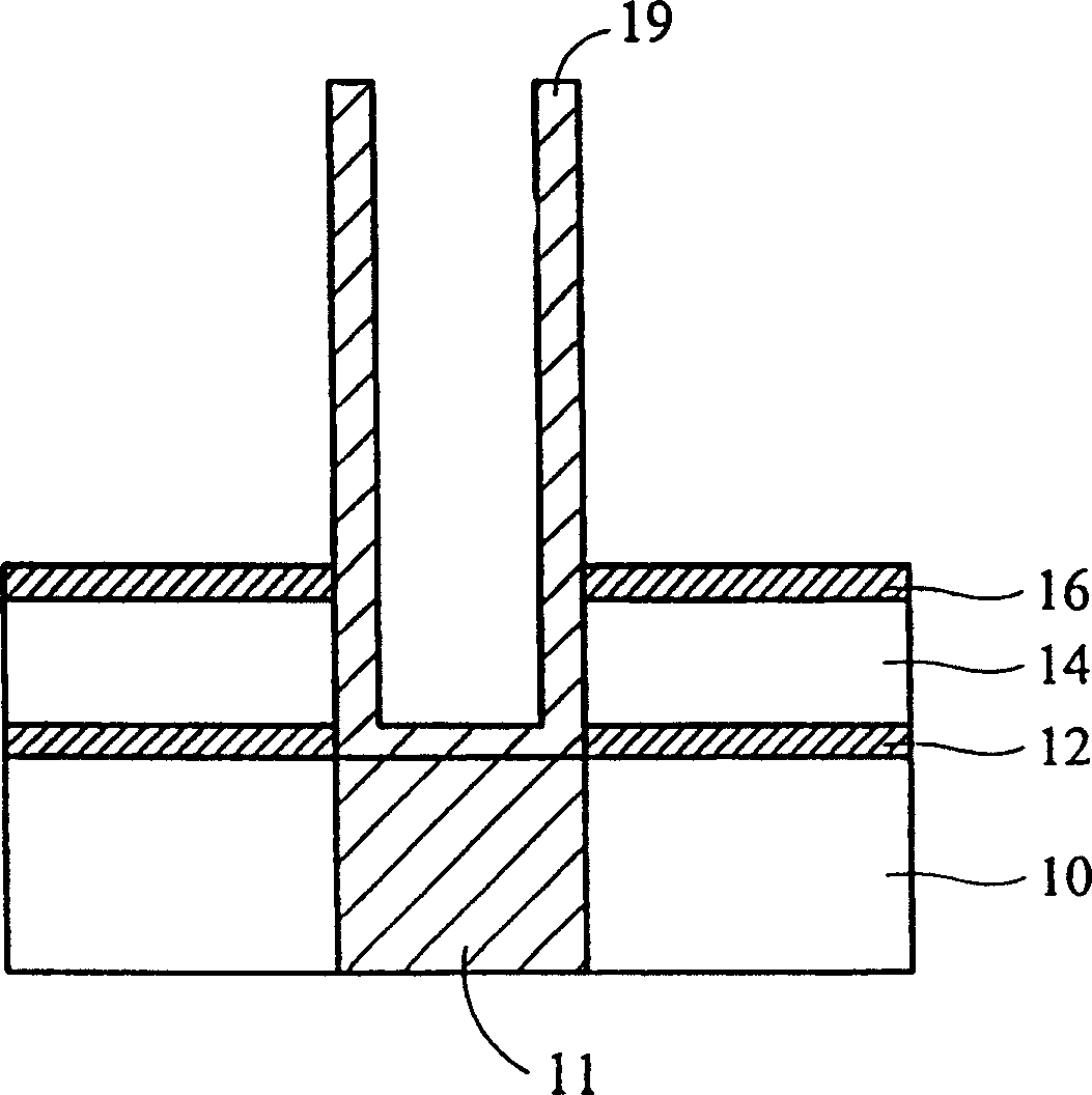
[0052] diagram 2-1 Illustrating the initial steps of the present invention, a silicon nitride layer 102 is formed on a semiconductor substrate 100 . The part below the silicon nitride layer 102 may contain several layers of metal interconnection or several semiconductor components that are electrically connected to each other, such as MOS transistors, resistors, logic components, etc. For the sake of convenience, the silicon nitride layer 102 The following semiconductor substrates and integrated circuit components are only denoted by reference numeral 100 . The method of the present invention is mainly applied to the LPCVD silicon nitride layer deposited at low temperature, and this silicon nitride layer is usually ...


PUM

PropertyMeasurementUnit
thicknessaaaaaaaaaa

Abstract

A method for decreasing the wet etching speed of silicon nitride includes implanting the nitrogen-containing ions into silicon nitride layer and thermal tempering to repair the damage caused by implanting and to generate Si-N bonds. It can increase the etching selectivity of silicon oxide to silicon nitrode, so using the silicon nitride layer as the etch terminating layer in LPCVD.

Description

technical field [0001] The invention relates to a semiconductor manufacturing technology, and in particular to a method for reducing the wet etching rate of silicon nitride. Background technique [0002] Silicon nitride (Si 3 N 4 ) is a common dielectric material in semiconductor manufacturing, and its main application is as an etching mask for silicon oxide layers (for example, in the process of self-aligned contact windows). In current semiconductor manufacturing, silicon nitride is mainly formed by Low Pressure Chemical Vapor Deposition (LPCVD) or Plasma Enhanced Chemical Vapor Deposition (PECVD). There is not much difference in the dry etching rate of the silicon nitride layer formed by the above two methods, but in terms of the wet etching rate, the PECVD silicon nitride layer is about 10 times faster than the LPCVD silicon nitride layer. [0003] Traditional LPCVD silicon nitride layers are usually made of SiH 2 Cl 2 with NH 3 For the deposition of reactants, the...

Claims


Application Information

Patent Timeline
Patent Type & Authority Patents(China)
IPC IPC(8): H01L21/285H01L21/3105H01L21/311H01L21/318H01L21/324
Inventor 周保华
Owner WINBOND ELECTRONICS CORP
Learn More