N type fin type field effect transistor and formation method thereof

A fin-type field effect and transistor technology, which is applied in the direction of semiconductor devices, semiconductor/solid-state device manufacturing, electrical components, etc., can solve the problems of transistor source-drain punch-through, etc., and achieve the enhanced ability to resist punch-through, prevent offset, and improve the resistance to punch-through The effect of the ability

Inactive Publication Date: 2016-03-30
SEMICON MFG INT (SHANGHAI) CORP
View PDF4 Cites 4 Cited by
  • Summary
  • Abstract
  • Description
  • Claims
  • Application Information

AI Technical Summary

Problems solved by technology

[0004] However, the existing fin field effect transistor

Method used


Image

  • N type fin type field effect transistor and formation method thereof
  • N type fin type field effect transistor and formation method thereof
  • N type fin type field effect transistor and formation method thereof

Examples


Embodiment Construction

[0033] As mentioned in the background, the fin field effect transistor formed in the prior art is prone to the problem of source-drain punch-through.

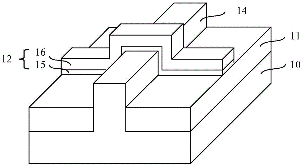
[0034] The study found that the reason why the fin field effect transistor in the prior art is prone to source-drain punch-through is that the fin field effect transistor has a raised fin, and the semiconductor substrate on both sides of the fin has an isolation structure, and the isolation structure covers the fin. Part of the sidewall surface of the portion and the surface of the isolation structure is lower than the top surface of the fin, the isolation structure is used for electrical isolation between the gate structure and the semiconductor and between adjacent fins, the gate structure spans the covering fin Part of the side and top surface of the fin, and part of the gate structure is located on the isolation structure, so the fin field effect transistor gate structure of the prior art only covers the upper region of the ...


PUM


Abstract

An N type fin type field effect transistor and a formation method thereof. The formation method of N type fin type field effect transistor includes the following steps: a semiconductor substrate is provided which has a protruding fin part, the fin part includes a bottom region and an upper region which are adjacent to each other, and the bottom region is located under the upper region; an ion implantation technology is performed, B ions and F ions are implanted into the fin part, and an implantation region is formed in the bottom region of the fin part; after the ion implantation technology, an annealing process is performed, the B ions and F ions in the implantation region are activated, and a doping region is formed in the bottom region of the fin part; after the annealing process is performed, a gate structure which stretches across and covers surfaces of side wall and top parts of the fin part is formed; and a source region and a drain region are formed in the fin part at two sides of the gate structure. The method provided by the invention improves a capability of resisting source leakage punchthrough of the fin type field effect transistor by preventing diffusion of boron ions in the doping region.

Description

technical field [0001] The invention relates to the field of semiconductor manufacturing, in particular to an N-type fin field effect transistor and a forming method thereof. Background technique [0002] MOS transistors generate switching signals by regulating the current through the channel region by applying a voltage to the gate. However, when the semiconductor technology enters the node below 32 / 28 nanometers, the control ability of the traditional planar MOS transistor to the channel current becomes weak, causing serious leakage current. Fin Field Effect Transistor (FinFET) is a new type of multi-gate device, which generally includes a semiconductor fin with a high aspect ratio, a gate structure covering part of the top and side walls of the fin, and a gate structure located on the gate. The source and drain regions in the fins on both sides of the structure, the gate structure of the fin field effect transistor can control the fins from the top and both sides, and ha...

Claims


Application Information

Patent Timeline
IPC IPC(8): H01L29/78H01L29/06H01L21/336
Inventor 居建华李勇
Owner SEMICON MFG INT (SHANGHAI) CORP
Why Eureka
Try Eureka