LED chip and manufacturing method thereof

A technology of LED chip and manufacturing method, applied in electrical components, circuits, semiconductor devices, etc., can solve problems such as uneven current density distribution, achieve uniform current density distribution, and improve luminous efficiency.

Inactive Publication Date: 2016-03-30
WUXI CHINA RESOURCES HUAJING MICROELECTRONICS
View PDF3 Cites 9 Cited by
  • Summary
  • Abstract
  • Description
  • Claims
  • Application Information

AI Technical Summary

Problems solved by technology

[0004] In view of this, an embodiment of the present invention provides an LED chip and its manufacturing method to solve the problem of uneven distribution of current density caused by the relatively concentrated flow of current between the P-type electrode and the N-type electrode in the prior art when the LED chip is working. technical issues

Method used


Image

  • LED chip and manufacturing method thereof
  • LED chip and manufacturing method thereof
  • LED chip and manufacturing method thereof

Examples


Embodiment 1

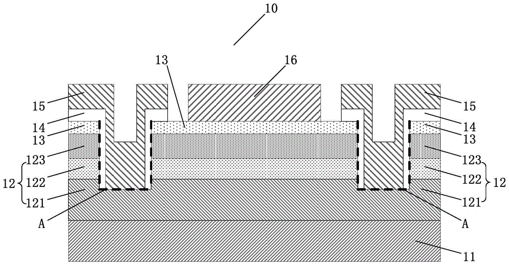
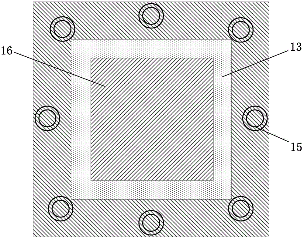
[0039] Embodiment 1 of the present invention provides an LED chip. figure 1 It is a schematic cross-sectional view of an LED chip provided by Embodiment 1 of the present invention. like figure 1 As shown, the LED chip 10 includes: a substrate 11; an epitaxial layer 12, the epitaxial layer 12 is located on the substrate 11; a transparent electrode layer 13, the transparent electrode layer 13 is located on the epitaxial layer 12; At least two grooves (shown in the area A surrounded by a dotted line in the figure), the grooves pass through the transparent electrode layer 13 in the longitudinal direction and the bottom is located in the epitaxial layer 12, and the grooves extend along the transparent electrode layer 13 edge distribution; insulating layer 14, the insulating layer 14 is lined on the side wall of the groove and the transparent electrode layer 13 on the edge of the groove; N-type electrode 15, the N-type electrode 15 is located on the insulating layer 14; and a P-ty...

Embodiment 2

[0059] Embodiment 2 of the present invention provides a method for manufacturing an LED chip. The manufacturing method of the LED chip in this embodiment can manufacture the LED chip described in the first embodiment above, and the manufacturing process is compatible with the existing process. In this embodiment, for the explanation of the concept and the detailed description of the working principle, please refer to Embodiment 1, which will not be repeated here.

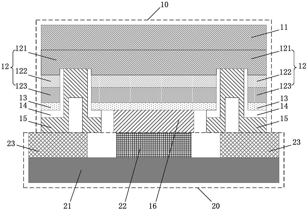
[0060] Figure 4 It is a schematic flow chart of a method for manufacturing an LED chip provided in Embodiment 2 of the present invention. like Figure 4 As shown, the manufacturing method of the LED chip of the present embodiment comprises:

[0061] Step 301, forming an epitaxial layer on the substrate;

[0062] In this step, further, forming an epitaxial layer on the substrate includes: sequentially forming an N-type GaN layer, an InGaN or GaN multi-quantum well active layer, and a P-type GaN layer on the subs...


PUM


Abstract

The invention discloses an LED chip and a manufacturing method thereof. The LED chip comprises a substrate; an epitaxial layer, which is arranged on the substrate; a transparency electrode layer, which is arranged on the epitaxial layer; at least two grooves, which vertically pass through the transparency electrode layer and the bottoms of which are arranged in the epitaxial layer, and which are distributed along the edge of the transparency electrode layer; an insulation layer, which is lined to the side walls of the grooves and on the transparency electrode layer at the edges of groove openings; N electrodes, which are arranged on the insulation layer; and a P electrode, which is arranged on the transparency electrode layer, wherein the distances between the P electrode and the N electrodes are same. The N electrodes of the LED chip encircle the P electrode, and the distances between the P electrode and the N electrodes are same, so that when the LED chip works, flow direction of the current between the N electrodes and the P electrode is allowed to be scattered, current density distribution is allowed to be more uniform, and luminous efficiency of the LED chip can be improved.

Description

technical field [0001] The embodiments of the present invention relate to the technical field of semiconductors, in particular to an LED chip and a manufacturing method thereof. Background technique [0002] Light Emitting Diode (LED for short) has the advantages of small size, long life, fast response, high direction controllability, good stability, low power consumption, no heat radiation, and no pollution sources of toxic substances such as mercury. Afterwards, its application and promotion are very rapid. [0003] With the application and promotion of LED, the development of LED-related technologies has also advanced by leaps and bounds, emerging in endlessly. At present, the structure of LED chips can be divided into vertical structure, front structure and flip structure. The flip-chip LED chip has good heat dissipation performance, so it has attracted the attention of technicians. In the prior art, when the LED chip is working, the current flow between the P-type el...

Claims


Application Information

Patent Timeline
Patent Type & Authority Applications(China)
IPC IPC(8): H01L33/38H01L33/20H01L33/00
CPCH01L33/38H01L33/00H01L33/20
Inventor 王磊朱琳王强
Owner WUXI CHINA RESOURCES HUAJING MICROELECTRONICS
Why Eureka
Try Eureka