Image sensor interlayer dielectric layer groove and method for forming image sensor

An interlayer dielectric layer, image sensor technology, applied in semiconductor/solid-state device manufacturing, electrical components, circuits, etc., can solve the problems of expensive, unfavorable photomasks, and reduce production costs, to eliminate the frame effect and save production costs. , the effect of improving performance

Active Publication Date: 2018-07-20
SHANGHAI HUAHONG GRACE SEMICON MFG CORP
View PDF3 Cites 0 Cited by
  • Summary
  • Abstract
  • Description
  • Claims
  • Application Information

AI Technical Summary

Problems solved by technology

[0007] However, the formation of the second groove 42 needs to re-make the photomask, and the price of the photomask is very expensive, which is not conducive to reducing the production cost

Method used


Image

  • Image sensor interlayer dielectric layer groove and method for forming image sensor
  • Image sensor interlayer dielectric layer groove and method for forming image sensor
  • Image sensor interlayer dielectric layer groove and method for forming image sensor

Examples


Embodiment Construction

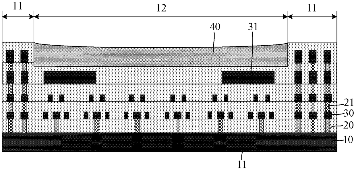
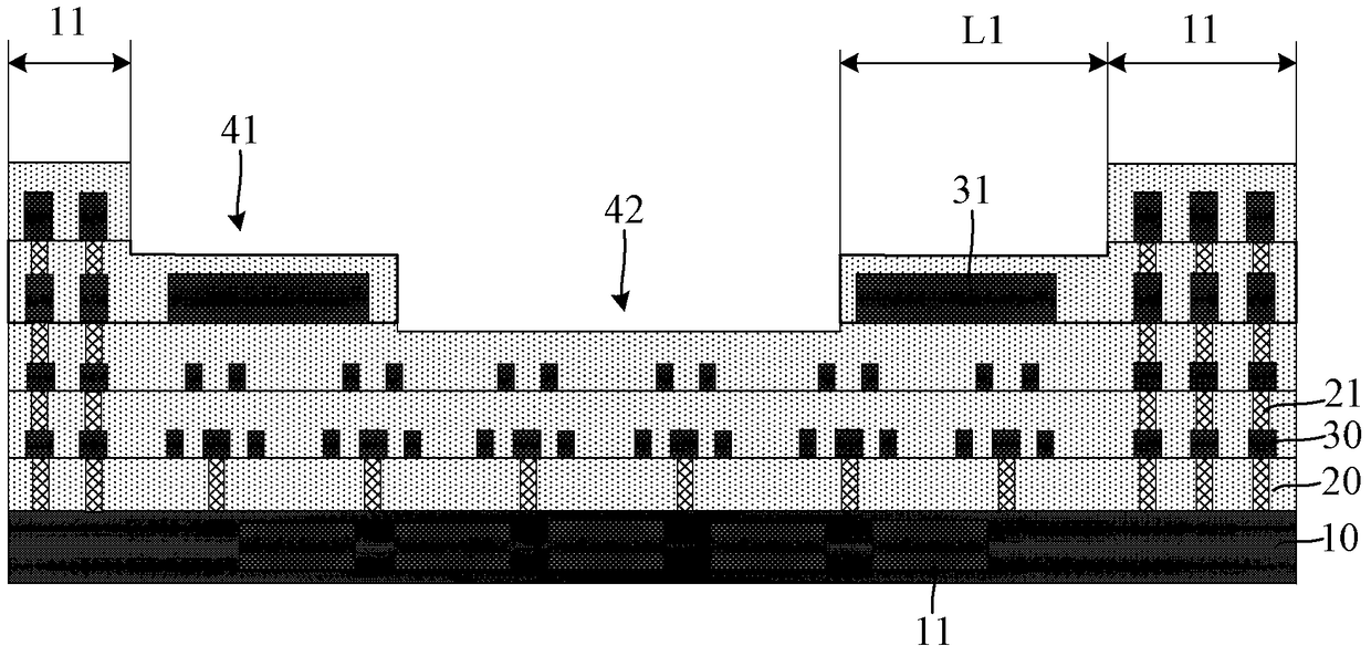
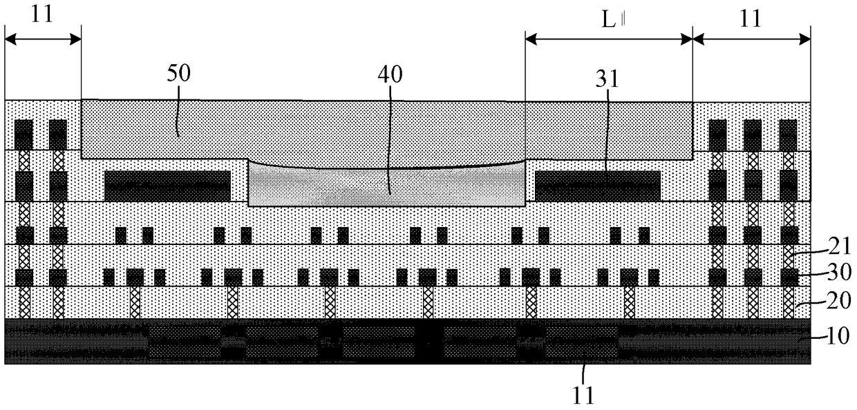
[0020] The method for forming the interlayer dielectric layer groove of the image sensor of the present invention will be described in more detail below in conjunction with schematic diagrams, wherein a preferred embodiment of the present invention is shown. It should be understood that those skilled in the art can modify the present invention described here, and The advantageous effects of the invention are still achieved. Therefore, the following description should be understood as the broad knowledge of those skilled in the art, but not as a limitation of the present invention.

[0021] In the interest of clarity, not all features of an actual implementation are described. In the following description, well-known functions and constructions are not described in detail since they would obscure the invention with unnecessary detail. It should be appreciated that in the development of any actual embodiment, numerous implementation details must be worked out to achieve the dev...


PUM


Abstract

The present invention provides a method for forming an image sensor interlayer dielectric layer trench and an image sensor. Primary etching is employed, with the etching shielding effect of two side light-blocking layers, and a second trench far from an edge area is formed in a last but one layer of interlayer dielectric layer. Only one type of light cover is needed by the primary etching, the second trench is formed without second etching, thus an additional light cover is not needed, and the production cost is saved. Further, a transparent lens is installed in the second trench, then a transparent encapsulating material is formed in the first trench, due to the controllable thickness of the encapsulating material, the thickness difference between a center area and the edge area can be reduced, a border effect is eliminated, and the performance of the formed image sensor is improved.

Description

technical field [0001] The invention relates to the field of semiconductor manufacturing, in particular to an image sensor interlayer dielectric layer groove and a method for forming the image sensor. Background technique [0002] Digital cameras are widely used electronic products today, and digital cameras contain image sensors. Image sensors, also known as photosensitive devices, are used to convert optical signals into electrical signals. They are the core and the most critical technology of digital cameras. Image sensors can be divided into charge-coupled device (Charge-Coupled Device) image sensors (commonly known as CCD image sensors) and CMOS (Complementary Metal Oxide Semiconductor) image sensors according to the principles they use, where CMOS image sensors are based on complementary metal oxide Semiconductor (CMOS) technology and manufacturing. Since the CMOS image sensor is manufactured using a traditional CMOS circuit process, the image sensor and its required ...

Claims


Application Information

Patent Timeline
Patent Type & Authority Patents(China)
IPC IPC(8): H01L27/146H01L21/311
Inventor 令海阳
Owner SHANGHAI HUAHONG GRACE SEMICON MFG CORP
Why Eureka
Try Eureka