
VDMOS device and manufacturing method thereof

A manufacturing method and device technology, which are applied in the fields of semiconductor/solid-state device manufacturing, semiconductor devices, electrical components, etc., can solve the problems of small threshold voltage adjustment range, etc., and achieve the effect of improving the adjustable range

Active Publication Date: 2016-04-06
FOUNDER MICROELECTRONICS INT
View PDF5 Cites 2 Cited by
  • Summary
  • Abstract
  • Description
  • Claims
  • Application Information

AI Technical Summary

Problems solved by technology

[0014] The purpose of the embodiments of the present invention is to provide a VDMOS device and its manufacturing method to solve the following problems in the prior art in adjusting the threshold voltage: when changing the thickness of the gate oxide layer, the adjustment range of the threshold voltage is small

Method used


Image

  • VDMOS device and manufacturing method thereof
  • VDMOS device and manufacturing method thereof
  • VDMOS device and manufacturing method thereof

Examples


Embodiment Construction

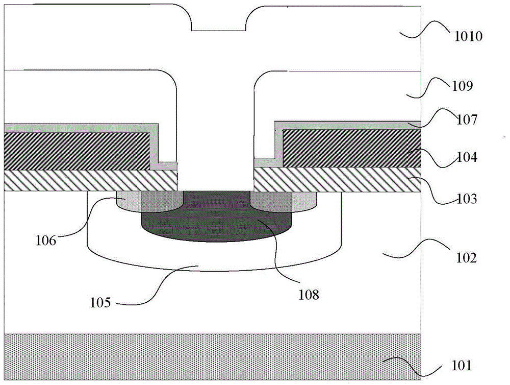
[0042] The VDMOS device and its manufacturing method provided by the present invention will be described in more detail below with reference to the accompanying drawings and embodiments.

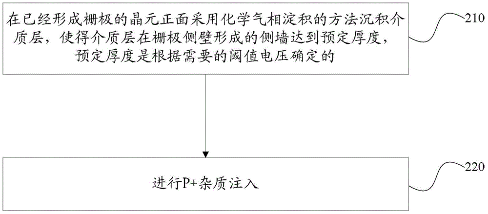
[0043] In the embodiment of the present invention, such as figure 2 As shown, the manufacturing method of VDMOS at least includes the following steps:

[0044] Step 210: Deposit a dielectric layer on the front of the wafer where the gate has been formed by chemical vapor deposition, so that the sidewall formed by the dielectric layer on the sidewall of the gate reaches a predetermined thickness. The predetermined thickness is determined according to the required threshold voltage.

[0045] Among them, the wafer is the carrier for making VDMOS devices. Wafer front side refers to the side used to form VDMOS devices.

[0046] Among them, there are many ways to realize the determination of the thickness of the sidewall according to the required threshold voltage. Here are some examples:

[...


PUM


Abstract

The embodiment of the invention discloses a VDMOS device and a manufacturing method thereof. The method comprises the steps that a dielectric layer is deposited on the front surface of a wafer on which a gate electrode is formed by adopting a chemical vapor deposition method so that the sidewalls of the dielectric layer formed on the side wall of the gate electrode are enabled to achieve preset thickness, and the preset thickness is determined according to the required threshold voltage; and every two opposite sidewalls act as mask film windows to perform P+ impurity injection. The VDMOS device with different threshold voltage can be manufactured according to the requirements so that adjustable range of threshold voltage can be enhanced, and increasing of channel resistance or early punchthrough of N+ / P- junctions does not occur.

Description

technical field [0001] The invention relates to the technical field of semiconductor chip manufacturing technology, in particular to a vertical double-diffused metal oxide semiconductor transistor (Verticial Double-diffused Metal Oxide Semiconductor, VDMOS) device and a manufacturing method thereof. Background technique [0002] VDMOS is a new generation of power electronic devices, mainly used in electronic switches, automotive electrical appliances, inverters, audio amplifiers and other fields. Threshold voltage is an important parameter of VDMOS performance, and is also an important control parameter in the manufacturing process of VDMOS devices. like figure 1 As shown, the cell structure of a planar VDMOS in the prior art: [0003] N-type semiconductor substrate 101; [0004] N-type epitaxial layer 102, formed on the surface of N-type semiconductor substrate 101; [0005] The P-body region 105 is located inside the N-type epitaxial layer 102; [0006] The P+ body re...

Claims


Application Information

Patent Timeline
Patent Type & Authority Applications(China)
IPC IPC(8): H01L29/78H01L29/06H01L21/336
CPCH01L29/1095H01L29/7802H01L29/66712
Inventor 刘竹
Owner FOUNDER MICROELECTRONICS INT
Learn More