A high-efficiency fpga technology mapping method

A mapping method and technology technology, applied in the computer field, can solve the problems of time-consuming technology mapping and unclear quality optimization of technology mapping, and achieve the effects of improving efficiency, reducing iterations, and optimizing efficiency

Active Publication Date: 2020-05-22
XIDIAN UNIV
View PDF2 Cites 0 Cited by
  • Summary
  • Abstract
  • Description
  • Claims
  • Application Information

AI Technical Summary

Problems solved by technology

Since ABC is a tool that pursues efficiency, and the quality optimization of technology mapping is time-consuming, ABC has to sacrifice quality in exchange for improving the efficiency of technology mapping, so the quality optimization of technology mapping by ABC is not obvious

Method used


Image

  • A high-efficiency fpga technology mapping method
  • A high-efficiency fpga technology mapping method
  • A high-efficiency fpga technology mapping method

Examples


Embodiment Construction

[0070] The present invention will be further described below in conjunction with the accompanying drawings. It should be noted that this embodiment is based on the technical solution, and provides detailed implementation and specific operation process, but the protection scope of the present invention is not limited to the present invention. Example.

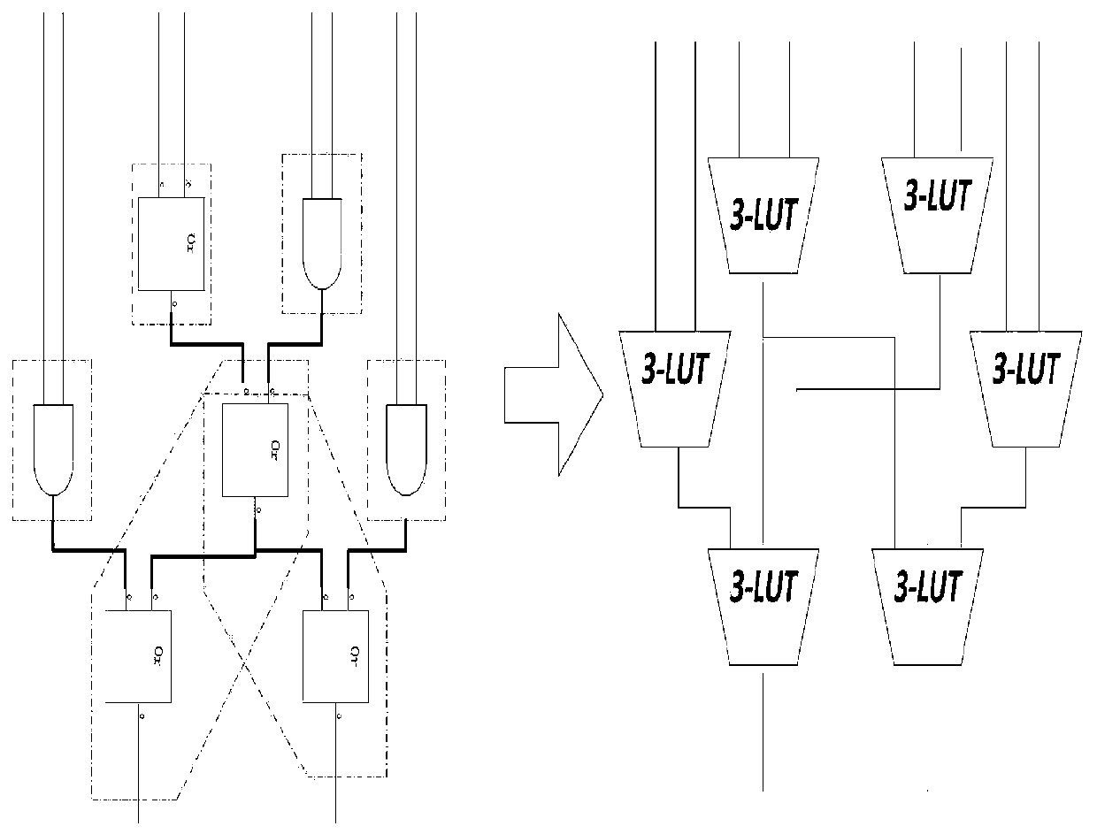
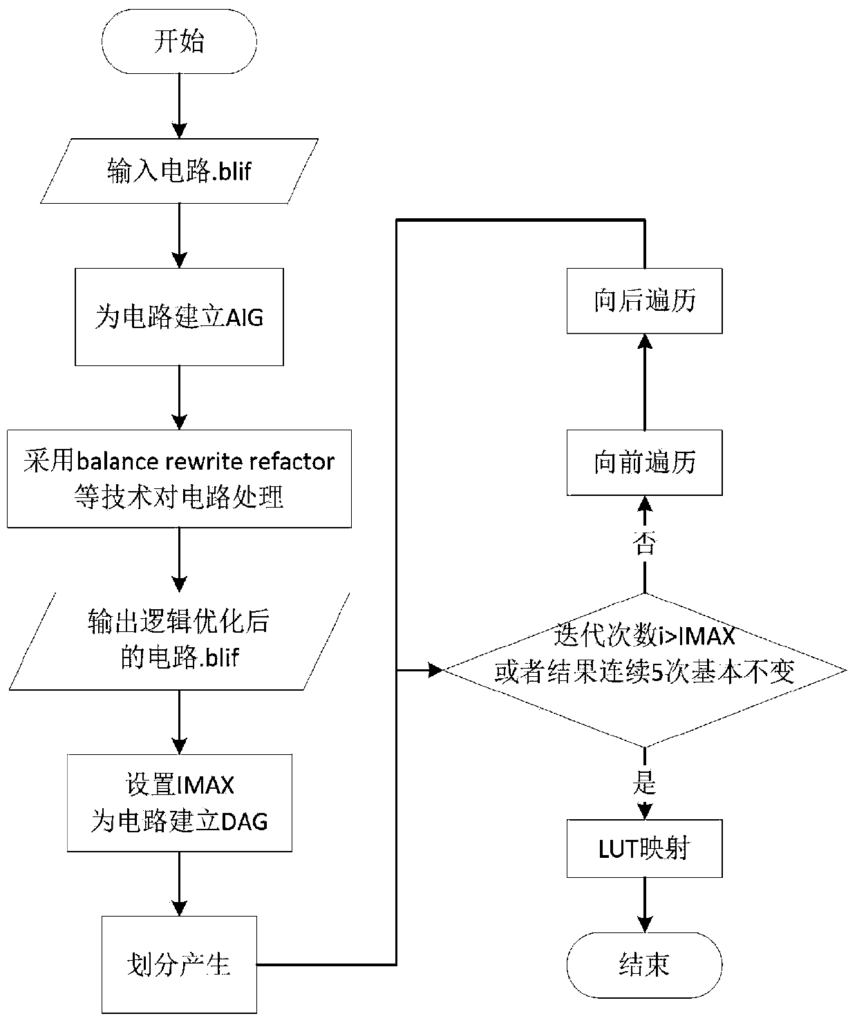
[0071] like figure 2 As shown, a high-efficiency FPGA technology mapping algorithm includes the following steps:

[0072] S1 logic optimization:

[0073] 1.1) Initialization: create an AIG diagram for the circuit;

[0074] 1.2) Decompose and optimize the AIG diagram obtained in step 1.1), obtain two input circuits and output;

[0075] S2 structure optimization:

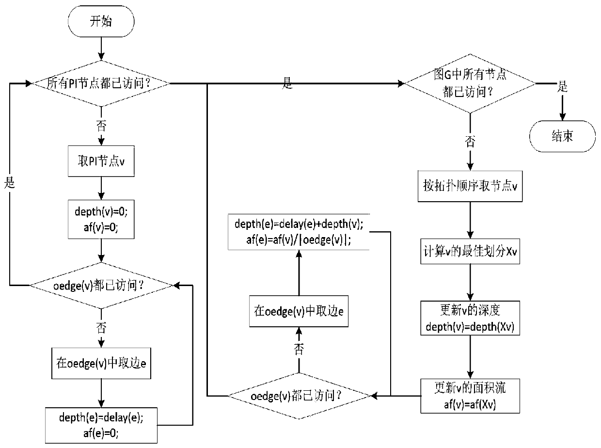
[0076] 2.1) Establish a DAG graph G for the circuit obtained after the logic optimization of step S1, and set the maximum number of iterations IMAX and the maximum number M of continuous execution results;

[0077] 2.2) Generate all k-feasible partitions for each ...


PUM


Abstract

The invention discloses an efficient FPGA technology mapping algorithm. Technical mapping is divided into logic optimization and structural optimization. The logic optimization part adopts an AIG model and technologies of balance, rewrite, refactor and the like to optimize a circuit. The structural optimization part adopts a DAG model and comprises three steps of partition generation, partition selection and LUT mapping. For the partition generation, a dynamic planning thought is adopted for quickly generating all k- feasible partitions for each node. For the partition selection, a partition set with a characteristic that a time delay and an area are optimized at the same time is finally selected through multi-time forward traversal and backward traversal iteration based on an iterative heuristic thought with an adaptively changeable iterative frequency. Meanwhile, a node area stream calculation formula is corrected and the randomness of the partition selection is improved. Through the LUT mapping, partition combination generated by the partition selection is mapped into an LUT network.

Description

technical field [0001] The invention relates to the field of computer technology, and can be used for the technical mapping problem of converting a gate-level network irrelevant to the circuit structure to a LUT network related to the circuit structure in the FPGA. Background technique [0002] In recent years, with the rapid development of integrated circuit technology, Field Programmable Gate Array (FPGA, Field Programmable Gate Array) has gained a lot of attention in digital system design because of its high integration, rich logic resources, flexible design and wide application range. Wide range of applications. [0003] The FPGA design process mainly includes design entry, behavioral synthesis, process mapping, packaging, placement and routing. Among them, as a key step in FPGA support software, technology mapping has attracted extensive research. [0004] The combination part of a Boolean circuit can be expressed as a DAG, G=(V(G), E(G)), V(G) and E(G) respectively r...

Claims


Application Information

Patent Timeline
Patent Type & Authority Patents(China)
IPC IPC(8): G06F30/343
CPCG06F30/331
Inventor 段振华杨凯强黄伯虎田聪张南王小兵
Owner XIDIAN UNIV
Why Eureka
Try Eureka