Semiconductor package with cooling fin, and packaging method for semiconductor package

A technology for semiconductors and heat sinks, applied in semiconductor devices, semiconductor/solid-state device manufacturing, semiconductor/solid-state device components, etc., can solve the problem of reducing the effective connection area of ​​the chip 2' source, reducing the effective utilization of product space, and operating procedures Complicated problems, to achieve the effect of increasing the effective welding surface, low cost, and reducing the operation process

Active Publication Date: 2016-04-13
ALPHA & OMEGA SEMICON CAYMAN
View PDF5 Cites 9 Cited by
  • Summary
  • Abstract
  • Description
  • Claims
  • Application Information

AI Technical Summary

Problems solved by technology

Therefore, processing the chip 2' leads to an increase in product cost, complicated work flow, and reduces the effective connect...

Method used


Image

  • Semiconductor package with cooling fin, and packaging method for semiconductor package
  • Semiconductor package with cooling fin, and packaging method for semiconductor package
  • Semiconductor package with cooling fin, and packaging method for semiconductor package

Examples


Embodiment Construction

[0027] The present invention will be further elaborated below by describing a preferred specific embodiment in detail in conjunction with the accompanying drawings.

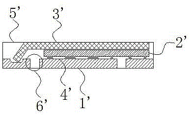
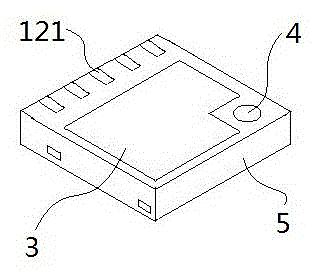
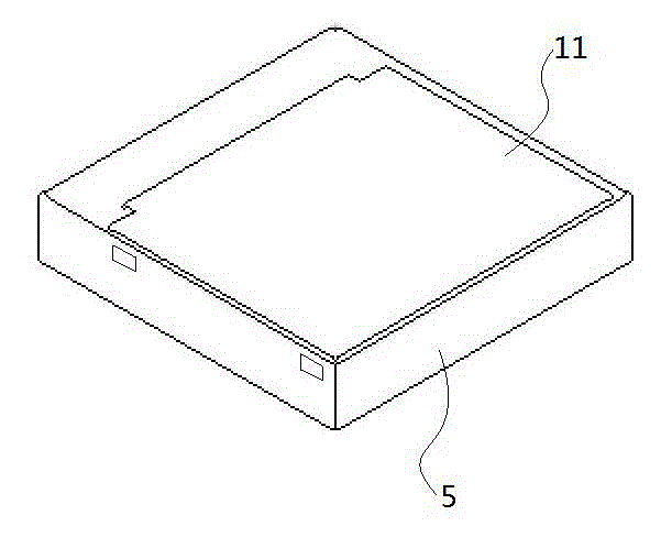
[0028] Such as Figure 2~Figure 5 shown, combined with Image 6 , a semiconductor package with a heat sink, comprising: a lead frame 1, the lead frame 1 includes a chip stage 11 and a plurality of pins 12 electrically connected to the chip stage 11 and bent, each pin 12 Including a pin surface 121 parallel to the loading table 11 and extending continuously without interruption between the loading table 11 and the pin surface 121;

[0029] A chip 2 is installed on the carrier stage 11, wherein the entire area of ​​the chip drain metal layer 201a that completely covers the first surface 201 of the chip is connected to the carrier stage 11, and the source metal layer 202a and the gate metal layer of the chip 2 202b is disposed on the second surface 202 of the chip opposite to the drain metal layer of the chip 2, a...


PUM


Abstract

The invention discloses a semiconductor package with a cooling fin, and the semiconductor package comprises a lead frame. The lead frame comprises a chip carrier and a plurality of bent pins, wherein the plurality of bent pins are electrically connected with the chip carrier, and each pin comprises a pin surface, is parallel to the chip carrier and continuously extends between the chip carrier and the pin surface. The semiconductor package also comprises a chip installed on the chip table; a source electrode metal piece and a grid electrode metal piece, which are arranged in an insulated and isolated manner, wherein one plane of the source electrode metal piece and one plane of the grid electrode metal piece are respectively connected with a source electrode metal layer and a grid electrode metal layer of the chip in an all-surface manner, and the opposite planes of the source electrode metal piece and the grid electrode metal piece share one plane with the pin surface; and a package body which enables the lead frame, the chip, the source electrode metal piece and the grid electrode metal piece to be packaged. The semiconductor package can increase the effective connection area of the source electrode, so as to reduce the conducting resistance and grounding resistance. The semiconductor package reduces the power loss, is low in cost, and is small in package size.

Description

technical field [0001] The invention relates to a semiconductor packaging technology, in particular to a semiconductor packaging with a heat sink and a packaging method thereof. Background technique [0002] Heat dissipation semiconductor packages in the prior art, such as figure 1 Shown: A chip 2' with surface treatment is flipped on the lead frame 1', and a copper sheet 3' is welded on the top again. After a special plastic packaging process, the copper sheet is exposed outside the plastic package 5'. After this process The top and bottom of the processed product have dual channels for heat dissipation. [0003] In the products in the prior art, the surface of the chip 2' needs to be treated, and the value ball 4' is used to prevent the overflow of the adhesive material under the chip 2', and a certain space 6' needs to be reserved between the bottom source and drain It is used to isolate the source and drain to prevent the short circuit between the source and the drain,...

Claims


Application Information

Patent Timeline
IPC IPC(8): H01L23/367H01L23/31H01L23/495H01L21/50H01L21/56
CPCH01L2224/32245
Inventor 霍炎牛志强魯明朕高洪涛
Owner ALPHA & OMEGA SEMICON CAYMAN
Why Eureka
Try Eureka