Single-layer circuit board, high-layer circuit board and fabrication method of high-layer circuit board
A production method and circuit board technology, which is applied in multi-layer circuit manufacturing, printed circuit manufacturing, printed circuit, etc., can solve the problems of resin filling ability influence, copper foil wrinkling, copper foil sinking, etc., to avoid local nonlinear expansion Shrinkage or deformation, sufficient glue flow, and smooth glue flow
- Summary
- Abstract
- Description
- Claims
- Application Information
AI Technical Summary
Problems solved by technology
Method used
Image
Examples
Embodiment 1
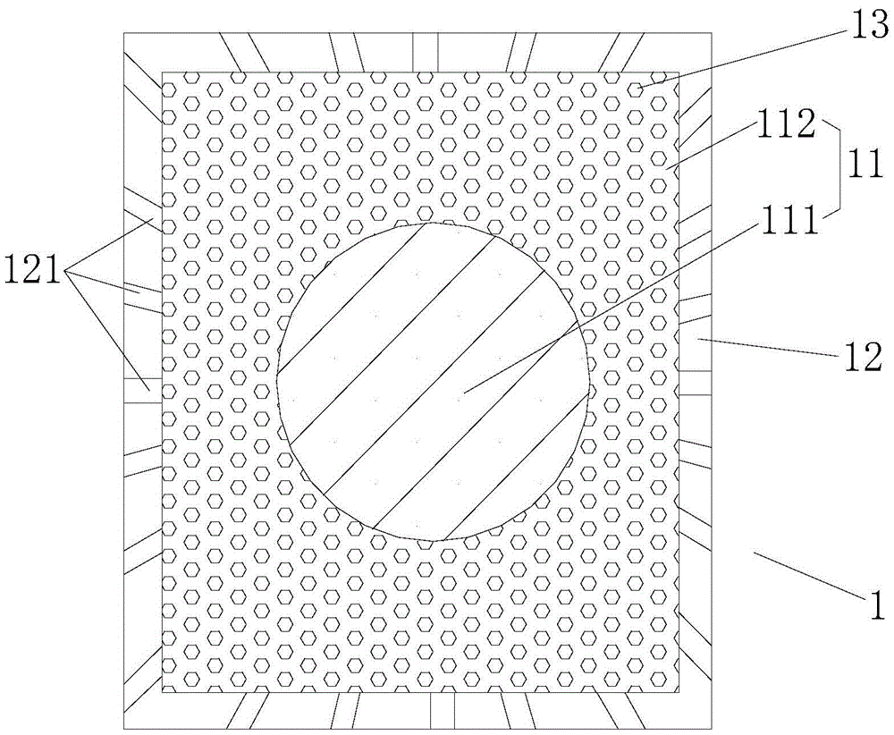
[0027] refer to figure 1 , a single-layer circuit board 1 described in this embodiment includes a core board 11 and a copper frame 12 arranged on the outer edge of the core board; The blank area 112 of the upper surface and the lower surface of the core board is provided with several evenly distributed pads 13, and there is a gap between adjacent pads 13; the upper surface of the copper frame 12 Several uniformly distributed glue guide grooves 121 are provided on the lower surface and the center line of the several glue guide grooves 121 intersects with the geometric center of the core plate 11 so that they can be arranged radially around the geometric center of the core plate 11.
[0028] A high-layer circuit board, comprising at least two or more laminated single-layer circuit boards 1 . The positions of the pads 13 between two adjacent single-layer circuit boards 1 are staggered along the lateral direction, so as to avoid overlapping of copper-free regions. The positions ...
Embodiment 2
[0036] The characteristics of this embodiment are: the diameter of the pads is 2 mm; on the same single-layer circuit board, the distance between adjacent pads is 0.87 mm, and the distance between centers is 2.87 mm. Others are the same as in Example 1.
Embodiment 3
[0038] The characteristics of this embodiment are: the diameter of the pads is 2 mm; on the same single-layer circuit board, the distance between adjacent pads is 0.87 mm, and the distance between centers is 2.87 mm. Others are the same as in Example 1.
[0039] Other examples:
[0040] The characteristics of the described embodiment are: the blank area 112 on the upper or lower surface of the core board is provided with several evenly distributed pads 13; the upper or lower surface of the copper frame 12 is provided with several evenly distributed The glue guide groove 12. Others are the same as in Example 1.
PUM
 Abstract
Description
Claims
Application Information
