3D nonvolatile memory, and manufacturing method and power consumption reduction method thereof

A non-volatile, manufacturing method technology, applied in static memory, read-only memory, semiconductor/solid-state device manufacturing, etc., can solve the problems of increased chip area, high production cost of 3D memory, and complexity of 3D memory chips. Low leakage power consumption, flexible implementation method, and the effect of reducing parasitic capacitance

Inactive Publication Date: 2016-04-20
SHANGHAI XINCHU INTEGRATED CIRCUIT
View PDF10 Cites 3 Cited by
  • Summary
  • Abstract
  • Description
  • Claims
  • Application Information

AI Technical Summary

Problems solved by technology

However, the use of DVFS technology requires the addition of many additional logic control circuits, which makes the ent

Method used


Image

  • 3D nonvolatile memory, and manufacturing method and power consumption reduction method thereof
  • 3D nonvolatile memory, and manufacturing method and power consumption reduction method thereof
  • 3D nonvolatile memory, and manufacturing method and power consumption reduction method thereof

Examples


Embodiment Construction

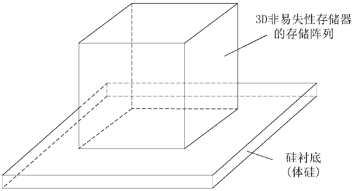
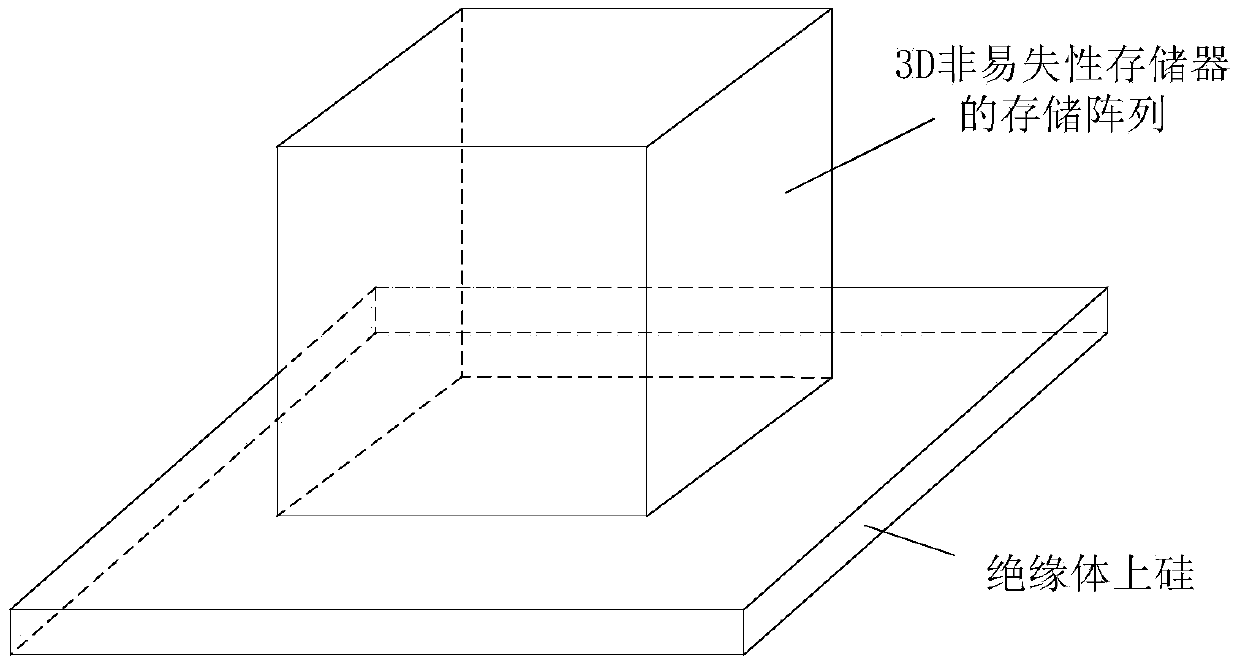
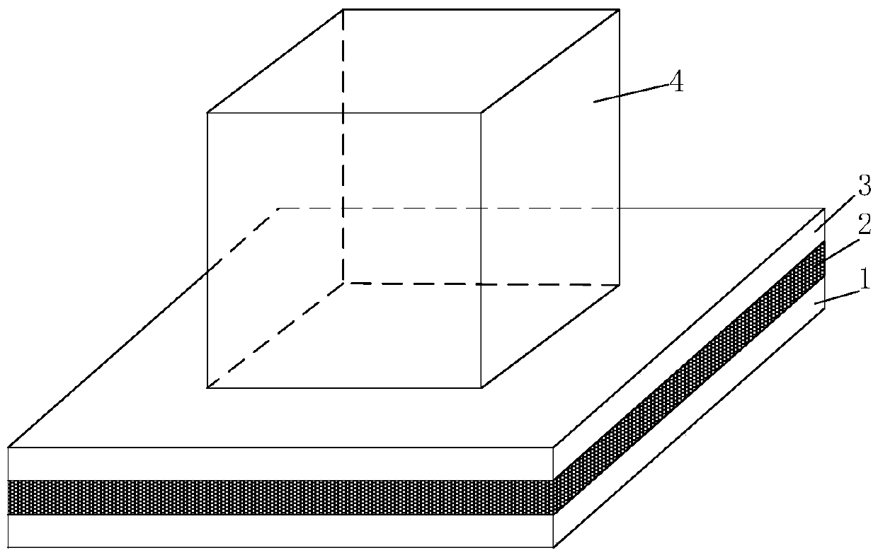
[0021] A specific embodiment of the 3D non-volatile memory based on the FDSOI process of the present invention is as follows image 3 shown. Among them, 1 is the silicon substrate (substrate); 2 is the buried oxide layer (BuriedOxideLayer, BOX), which acts as an insulating layer between 1 and 3; 3 is the top layer of monocrystalline silicon, which is used to realize the periphery of the 3D non-volatile memory CMOS logic circuit; 4 is a storage array of 3D non-volatile memory.

[0022] Furthermore, in the present invention, the performance and power consumption of different functional modules can be optimized by adjusting the back gate voltage. By adjusting the back gate voltage, the turn-on voltage of the transistor can be lowered, so that the transistor can work normally at a lower voltage, and can even work normally near the threshold voltage (near-Vt), so the power consumption of the chip will be greatly reduced . Such as Figure 4 What is shown is the peripheral CMOS l...


PUM


Abstract

The invention discloses an FDSOI-process-based 3D nonvolatile memory, and a manufacturing method. The 3D nonvolatile memory comprises a silicon substrate, a buried oxide layer, a monocrystalline silicon top layer and a 3D nonvolatile memory storage array. The buried oxide layer serves as an insulation layer of the first layer and the third layer. The monocrystalline silicon top layer is used for realizing a peripheral CMOS logic circuit of the 3D nonvolatile memory. According to the invention, the two parts, being the 3D nonvolatile memory storage array and the peripheral CMOS logic circuit of the D nonvolatile memory, of the FDSOI-process-based 3D nonvolatile memory can be produced by different manufacturing works. The performances and power consumption of the 3D nonvolatile memory can be optimized by adjusting back gate voltages of different functional modules. The break-over voltage of the transistor can be reduced by adjusting the back gate voltages, so that the transistor can work normally under a lower voltage and even can work normally under a voltage close to a threshold voltage and thus the chip power consumption can be substantially reduced.

Description

technical field [0001] The invention relates to a 3D nonvolatile memory, in particular to a 3D nonvolatile memory based on an FDSOI process, a manufacturing method thereof, and a method for reducing power consumption. Background technique [0002] As the process nodes become smaller and smaller, the miniaturization process of memory chips is facing its limit. In order to obtain higher storage density and read speed, major manufacturers have gradually invested in the development of 3D memory technology. The feature of 3D memory technology is not realized by chip stacking or 3D packaging, but the storage unit adopts 3D technology. For example, in the traditional planar NAND flash memory, the floating gate transistor of the storage unit is a planar transistor, and all the source terminals and the drain terminals are located on the same plane, while the 3D-NAND storage unit uses a three-dimensional transistor, and the source terminals and the drain terminals are respectively in...

Claims


Application Information

Patent Timeline
IPC IPC(8): H01L27/115H01L21/8247G11C16/34H01L27/11521H01L27/11551H01L27/11568H01L27/11578
CPCG11C16/3495H10B69/00
Inventor 景蔚亮陈邦明
Owner SHANGHAI XINCHU INTEGRATED CIRCUIT
Why Eureka
Try Eureka