Semiconductor device and fabrication methods thereof

A semiconductor and device technology, applied in the field of semiconductor devices, can solve problems such as horizontal channel reduction and short channel effect

Active Publication Date: 2016-04-20
SAMSUNG ELECTRONICS CO LTD
View PDF3 Cites 17 Cited by
  • Summary
  • Abstract
  • Description
  • Claims
  • Application Information

AI Technical Summary

Problems solved by technology

However, when a semiconductor device has a two-dimensional (2D) planar structure, as the size of the semicondu...

Method used


Image

  • Semiconductor device and fabrication methods thereof
  • Semiconductor device and fabrication methods thereof
  • Semiconductor device and fabrication methods thereof

Examples


Embodiment Construction

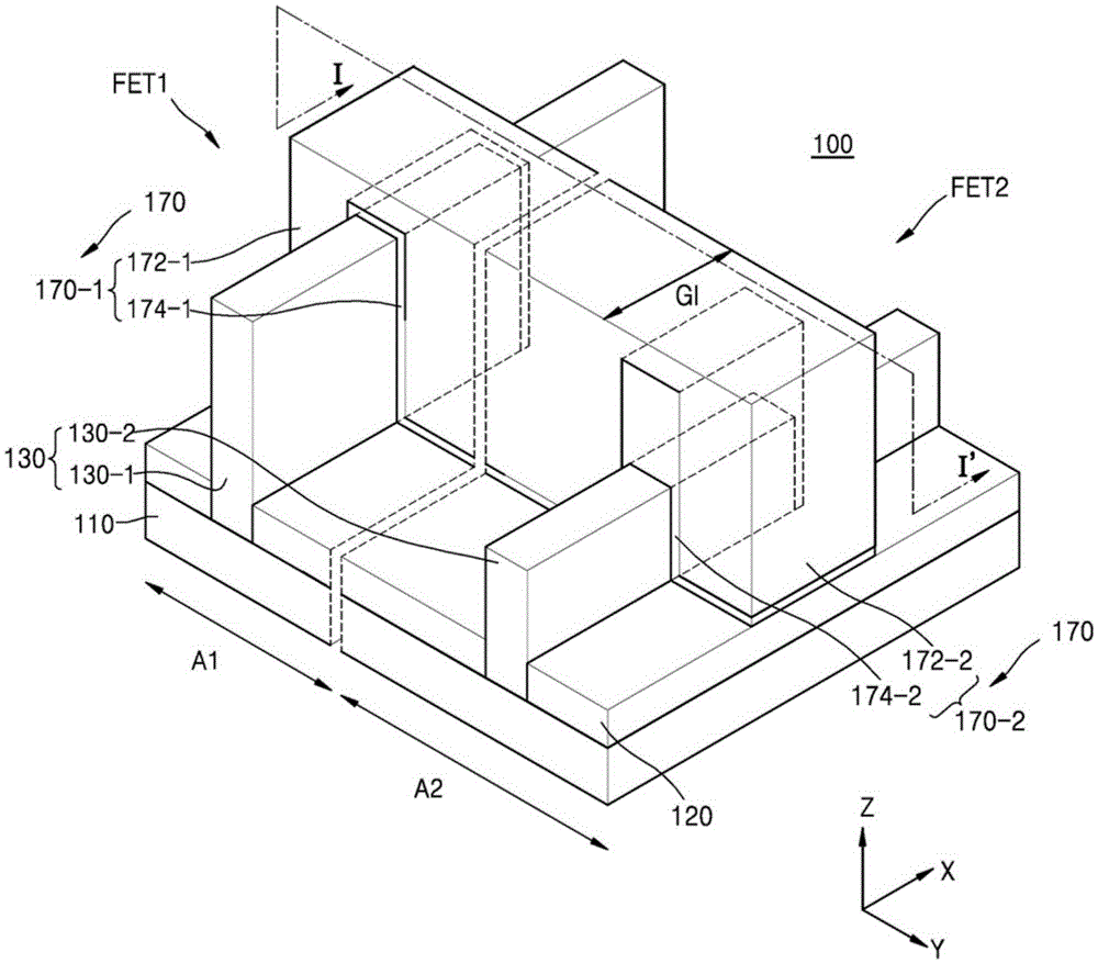
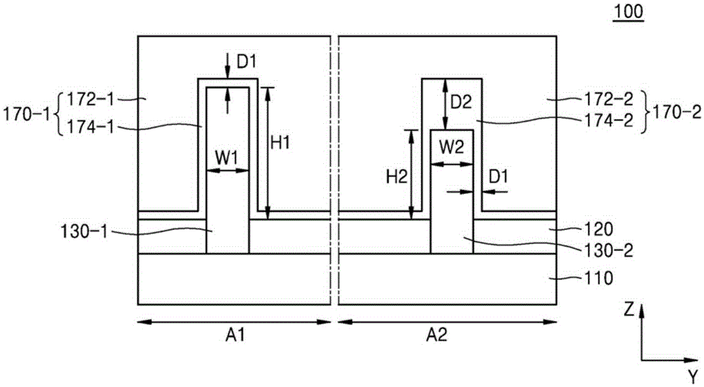
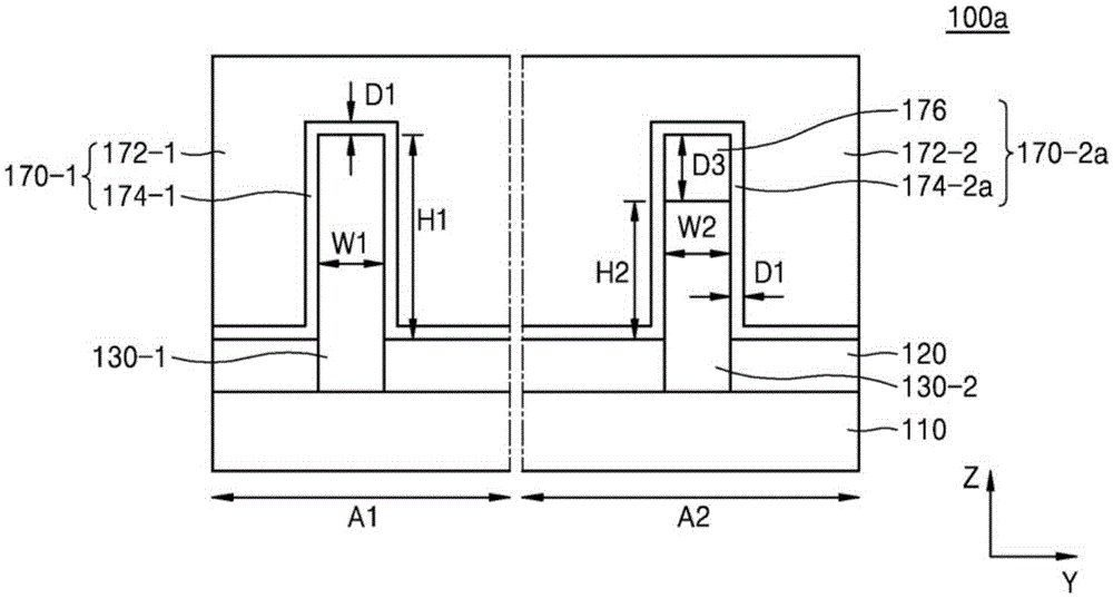
[0043] Hereinafter, the inventive concept will be described more fully with reference to the accompanying drawings, in which elements of the inventive concept are shown. Inventive concepts may, however, be embodied in many different forms and should not be construed as limited to the example embodiments set forth herein. Rather, these embodiments are provided so that this disclosure will be thorough and complete, and will fully convey the scope of the inventive concept to those skilled in the art. Throughout the specification, the same reference numerals denote the same parts. For convenience of description and clarity, structures or sizes of elements in the drawings are exaggerated, and components not related to the detailed description are omitted in the drawings. The terms used herein are for describing example embodiments only and are not intended to be limiting of example embodiments.

[0044] It will be understood that when an element or layer is referred to as being "...


PUM


Abstract

The invention provides a semiconductor device and fabrication methods thereof. The semiconductor device includes a substrate having a logic device region including logic devices thereon, and an input/output (I/O) device region including I/O devices thereon adjacent the logic device region. A first fin field-effect transistor (FinFET) on the logic device region includes a first semiconductor fin protruding from the substrate, and a triple-gate structure having a first gate dielectric layer and a first gate electrode thereon. A second FinFET on the I/O device region includes a second semiconductor fin protruding from the substrate, and a double-gate structure having a second gate dielectric layer and a second gate electrode thereon. The first and second gate dielectric layers have different thicknesses. Related devices and fabrication methods are also discussed.

Description

technical field [0001] The inventive concepts relate to semiconductor devices, and more particularly, to semiconductor devices including a field effect transistor (FET) having a fin structure and a method of manufacturing the same. Background technique [0002] Semiconductor devices are reduced in size to form large-capacity, high-performance, and highly-integrated devices. For example, in order to increase the degree of integration of semiconductor devices per unit area, the density of semiconductor devices can be increased by reducing the size of semiconductor devices and reducing the spacing between semiconductor devices. However, when the semiconductor device has a two-dimensional (2D) planar structure, as the size of the semiconductor device decreases, the length of the horizontal channel may decrease, and thus the short channel effect may occur. In order to reduce or prevent such short channel effects, FinFETs with vertical fin structures can be used. Due to the stru...

Claims


Application Information

Patent Timeline
IPC IPC(8): H01L29/78H01L29/06H01L21/336
CPCH01L29/0603H01L29/0684H01L29/0688H01L29/66484H01L29/66795H01L29/7855H01L29/7856H01L21/823412H01L21/823431H01L21/845H01L29/7853H01L27/0886H01L27/1211H01L29/785
Inventor 郑恩爱崔正达中西俊郎金有彬南甲镇李同规焦广泛
Owner SAMSUNG ELECTRONICS CO LTD
Why Eureka
Try Eureka