
A low-voltage transparent oxide thin film transistor and its preparation method

A transparent oxide and thin-film transistor technology, which is applied in transistors, semiconductor/solid-state device manufacturing, circuits, etc., can solve the problem of not meeting the requirements of large-screen display for process uniformity and consistency, complex p-SiTFT technology, and opaque LTPSTFT and other issues, to achieve the effect of improving device mobility, low price, and good transparency

Active Publication Date: 2018-05-29
HENAN UNIVERSITY
View PDF3 Cites 0 Cited by
  • Summary
  • Abstract
  • Description
  • Claims
  • Application Information

AI Technical Summary

Problems solved by technology

However, the current LTPS technology cannot meet the uniformity and consistency requirements of the large-screen display process, so it is mainly for the application of small and medium-sized display screens
In addition, the preparation process of LTPS is relatively complicated and the high production cost also restricts the wider application of LTPS TFT. The p-Si TFT technology also has the disadvantages of complex process, expensive equipment, and high cost, and its process temperature is still too high for organic substrates. , cannot meet the needs of flexible display, and LTPS TFT is not transparent, which seriously hinders its application in the field of flexible display and transparent display

Method used


Image

  • A low-voltage transparent oxide thin film transistor and its preparation method
  • A low-voltage transparent oxide thin film transistor and its preparation method
  • A low-voltage transparent oxide thin film transistor and its preparation method

Examples


Embodiment 1

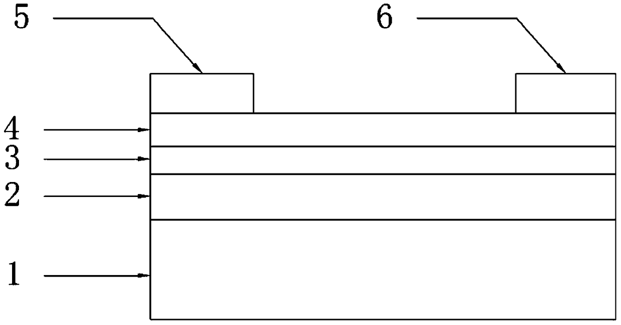
[0046] The low-voltage transparent oxide thin film transistor of this embodiment has a bottom-gate and top-electrode structure, such as figure 1 As shown, from bottom to top include:

[0047] The substrate 1 is ITO conductive glass; the upper conductive film of the ITO conductive glass is an ITO gate electrode 2;

[0048] The gate electrode insulating layer 3 is transparent ZrO 2 a film located on the ITO gate electrode 2;

[0049] The active layer 4 is a transparent oxide film located on the gate electrode insulating layer 3;

[0050] The source electrode 5 and the drain electrode 6 are both transparent tin oxide doped indium oxide (ITO) films, and are respectively located on the active layer 4 .

[0051] Wherein, the transparent oxide film is an indium-doped zinc oxide (InZnO) film; in the transparent oxide film, the mass percentage of indium is 3%; the transparent ITO (tin oxide-doped indium oxide) film Among them, the mass ratio of indium oxide to tin oxide is 90:10. ...

Embodiment 2

[0066] The low-voltage transparent oxide thin film transistor of this embodiment has a bottom-gate and top-electrode structure (the structure is the same as that of Embodiment 1), and sequentially includes from bottom to top:

[0067] The substrate is ITO conductive glass; the upper conductive film of the ITO conductive glass is an ITO gate electrode;

[0068] Gate electrode insulating layer, transparent ZrO 2 a film on the ITO gate electrode;

[0069] an active layer, which is a transparent oxide film, located on the gate electrode insulating layer;

[0070] The source electrode and the drain electrode are both transparent tin oxide doped indium oxide (ITO) films, respectively located on the active layer.

[0071] Wherein, the transparent oxide film is a titanium doped zinc oxide (TiZnO) film; in the transparent oxide film, the mass percentage of titanium is 1%; the transparent ITO (tin oxide doped indium oxide) film Among them, the mass ratio of indium oxide to tin oxide ...

Embodiment 3

[0086] The low-voltage transparent oxide thin film transistor of this embodiment has a bottom-gate and top-electrode structure (the structure is the same as that of Embodiment 1), and sequentially includes from bottom to top:

[0087] The substrate is ITO conductive glass; the upper conductive film of the ITO conductive glass is an ITO gate electrode;

[0088] Gate electrode insulating layer, transparent ZrO 2 a film on the ITO gate electrode;

[0089] an active layer, which is a transparent oxide film, located on the gate electrode insulating layer;

[0090] The source electrode and the drain electrode are both transparent tin oxide doped indium oxide (ITO) films, respectively located on the active layer.

[0091] Wherein, the transparent oxide film is a gallium-doped zinc oxide (GaZnO) film; in the transparent oxide film, the mass percentage of gallium is 5%; the transparent ITO (tin oxide-doped indium oxide) film Among them, the mass ratio of indium oxide to tin oxide is...


PUM


Abstract

The invention discloses a low-voltage transparent oxide thin film transistor and a preparation method thereof. The thin film transistor comprises a substrate, a gate electrode insulating layer, an active layer, a source electrode and a drain electrode, wherein the substrate is a piece of ITO conductive glass, an upper ITO conductive film on the ITO conductive glass is an ITO gate electrode, the gate electrode insulating layer is a transparent ZrO2 film and is disposed on the ITO gate electrode, the active layer is a transparent oxide film and is disposed on the gate electrode insulating layer, and the source electrode and the drain electrode are transparent ITO films and are disposed on the active layer. According to the transparent oxide thin film transistor, as the gate electrode insulating layer is a ZrO2 film with high dielectric constant, full transparency and low-voltage switching-on characteristics of the thin film transistor are achieved, the thin film transistor is of high switching ratio and carrier mobility, and the thin film transistor has a broad application prospect in flat display, transparent electronic devices, flexible display and other fields. By using the thin film transistor as a pixel switch, the opening ratio of an active matrix is improved greatly, the brightness is improved, and the power consumption is reduced.

Description

technical field [0001] The invention belongs to the technical field of thin film transistors, in particular to a low-voltage transparent oxide thin film transistor, and also to a preparation method of the low-voltage transparent oxide thin film transistor. Background technique [0002] A thin film transistor (Thin Film Transistor, TFT for short) is an active device, which is used as a switching control device in a liquid crystal display (LCD) due to its low turn-on voltage and high on / off current ratio. Thin-film transistor (TFT) is the core device of flat-panel display, and any active-matrix-addressed flat-panel display depends on TFT control and drive. Since the pixels in TFT-LCD are controlled by corresponding TFTs, in order to adapt to the development of large-area, high-quality, low-cost and high-reliability flat-panel displays, the requirements for TFT devices are getting higher and higher. The performance of the TFT is related to the carrier mobility of the material ...

Claims


Application Information

Patent Timeline
Patent Type & Authority Patents(China)
IPC IPC(8): H01L29/786H01L21/34
CPCH01L29/66969H01L29/7869
Inventor 张新安赵俊威李爽张伟风
Owner HENAN UNIVERSITY
Learn More