
Reconfigurable multi-stack inductor

A technology of inductors and inductance values, applied in the field of on-chip inductor components

Active Publication Date: 2016-05-04
IBM CORP
View PDF10 Cites 4 Cited by
  • Summary
  • Abstract
  • Description
  • Claims
  • Application Information

AI Technical Summary

Problems solved by technology

However, existing inductor structures still occupy the same space on the chip or semiconductor substrate whether or not one or more inductors are coupled to produce different inductance values

Method used


Image

  • Reconfigurable multi-stack inductor
  • Reconfigurable multi-stack inductor
  • Reconfigurable multi-stack inductor

Examples


Embodiment Construction

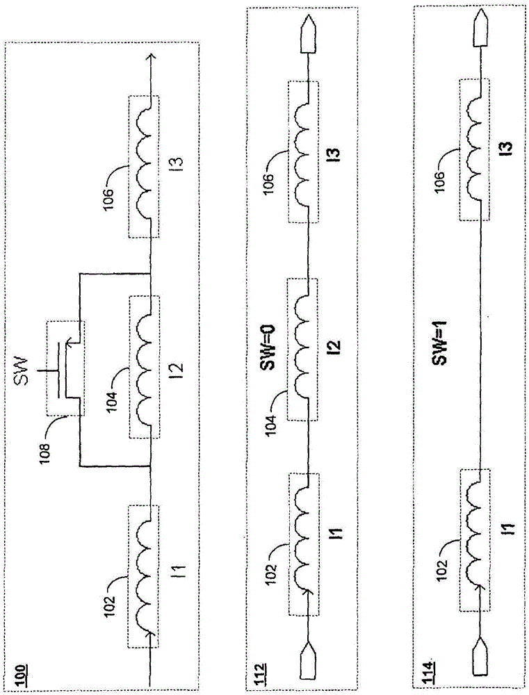
[0015] Exemplary embodiments described below are directed to moderately-Q reconfigurable on-chip programmable circuits operable to provide increased tuning range (e.g., ~40%) while maintaining a reduced footprint within the chip (e.g., semiconductor device). Refactor the inductor component.

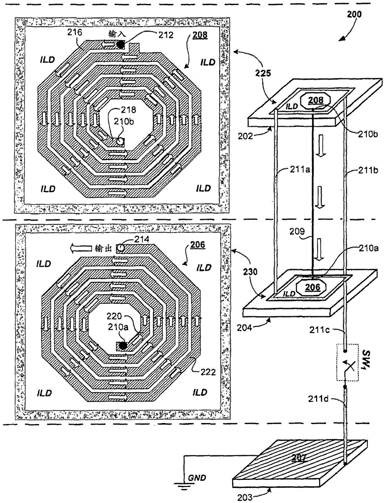
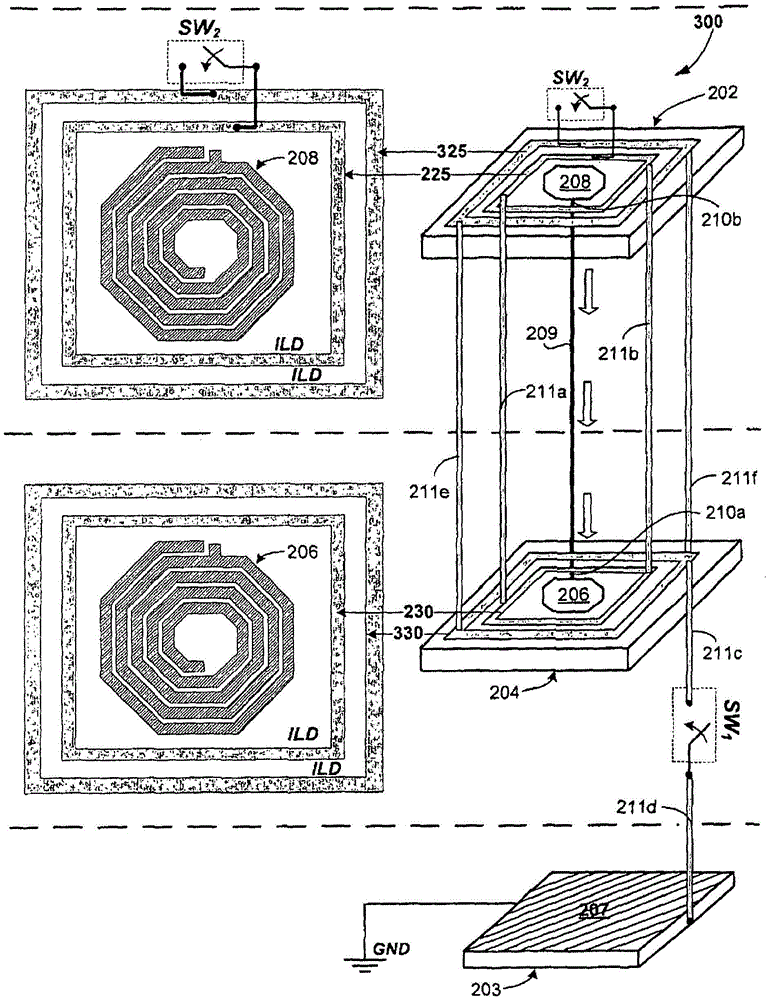
[0016] figure 2 An exemplary embodiment of a reconfigurable on-chip stacked inductor 200 is depicted. The depicted reconfigurable on-chip stack inductor 200 may be fabricated on three metal layers 202 , 203 , 204 , eg corresponding to the backend of the line (BEOL) region of a semiconductor device. A first inductor, such as a first conductive spiral trace structure 206 (ie, coil), is formed in metal layer 204, while a second inductor, such as a second conductive spiral trace structure 208 (ie, coil) is formed in metal layer 202 . The first conductive spiral trace structure 206 (i.e., inductor structure 206) is electrically coupled to the second conductive spiral trace structure 208 (i....


PUM

PropertyMeasurementUnit
Thicknessaaaaaaaaaa

Abstract

A reconfigurable multi-stack inductor formed within a semiconductor structure may include a first inductor structure located within a first metal layer of the semiconductor structure, a first ground shielding structure located within the first metal layer that is electrically isolated from and circumferentially bounds the first inductor structure, and a second inductor structure located within a second metal layer of the semiconductor structure, whereby the second inductor structure is electrically coupled to the first inductor structure. A second ground shielding structure located within the second metal layer is electrically isolated from and circumferentially bounds the second inductor structure, whereby the first and second inductor generate a first inductance value based on the first ground shielding structure and second ground shielding structure being coupled to ground, and the first and second inductor generate a second inductance value based on the first ground shielding structure and second ground shielding structure electrically floating.

Description

technical field [0001] The present invention relates generally to semiconductor devices, and in particular to on-chip inductor assemblies. Background technique [0002] Many communication systems can be implemented on a single chip. With the increasing demand for personal mobile communications, integrated semiconductor devices such as complementary metal-oxide-semiconductor (CMOS) devices may include, for example, voltage-controlled oscillators (VCOs), low-noise amplifiers (LNAs), tuned radio receiver circuits, or power Amplifier (PA). However, each of these VCO, LNA, PA and tuned radio receiver circuits may require an on-chip inductor component in its circuit design. Therefore, there will be a need for high quality, variable on-chip inductor devices. [0003] Several design considerations associated with forming an on-chip inductor assembly may include, for example, quality factor (i.e., Q-factor), self-resonant frequency (f SR ), cost considerations affected by the are...

Claims


Application Information

Patent Timeline
IPC IPC(8): H01F21/12H01L23/64
CPCH01F17/0013H01F27/2871H01F27/289H01F2017/008H01L2924/0002H01F27/2804H01F2027/2809Y10T29/4902H01F27/36H01F27/363H01L2924/00H01F41/041H01L23/645H01L23/60
Inventor 孙频平裴成文徐铮
Owner IBM CORP
Learn More