Wafer test data processing method and system

A test data and wafer test technology, applied in the direction of electrical digital data processing, special data processing applications, instruments, etc., can solve the problem of low efficiency of data upload, backup and deletion, low utilization of storage resources, and low data processing effect To improve processing performance, avoid dependencies, and ensure timeliness and accuracy

Active Publication Date: 2016-05-11
SEMICON MFG INT (SHANGHAI) CORP +1
View PDF8 Cites 7 Cited by
  • Summary
  • Abstract
  • Description
  • Claims
  • Application Information

AI Technical Summary

Problems solved by technology

[0006] The storage method of wafer test data is stored by point, that is, the test result of a wafer test data parameter of a chip (Die) on a wafer (wafer) is stored in the database as a record, and a wafer generates The number of records is the number of chips multiplied by the number of wafer test parameters, and the efficiency of data upload, backup and deletion is not high
[0007] The wafer test data monitoring system obtains the original wafer test data from the database and performs calculations. Due to the limitation of the data storage method, the data processing effect is not good and the performance is not high
[0008] The method of directly storing wafer test data into the database results in low utilization of storage resources and high IT costs

Method used


Image

  • Wafer test data processing method and system
  • Wafer test data processing method and system
  • Wafer test data processing method and system

Examples


Embodiment Construction

[0060] The specific embodiment of the present invention will be further described below in conjunction with accompanying drawing:

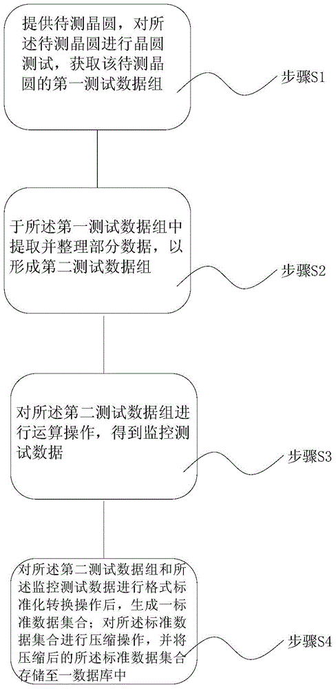
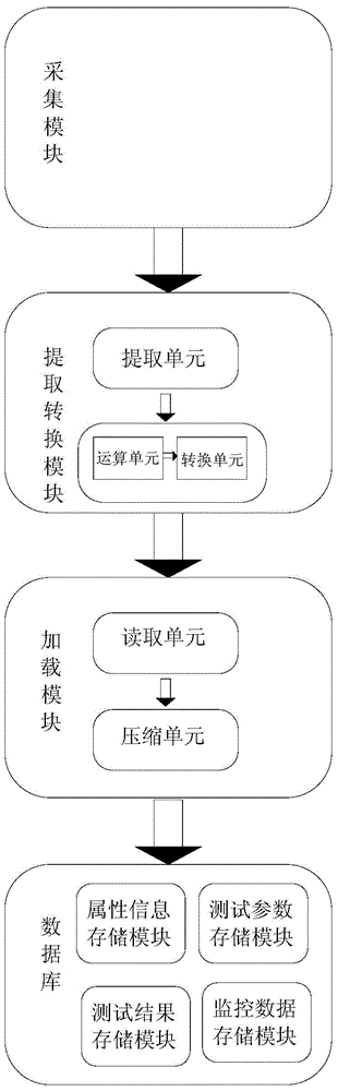
[0061] figure 1 It is a flowchart of a method for processing wafer test data provided by the present invention, such as figure 1 As shown, this embodiment relates to a method for processing wafer test data, which specifically includes the following steps;

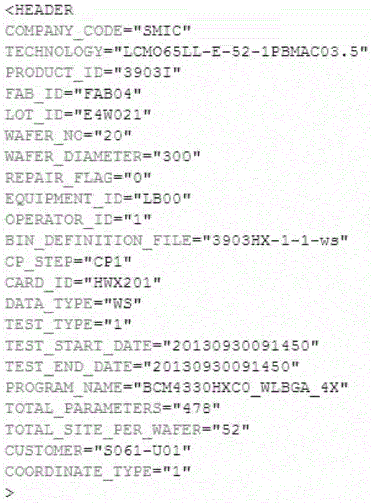
[0062] Step S1: Provide a wafer to be tested, and perform a wafer test on the wafer to be tested, and obtain a first test data set of the wafer to be tested. Preferably, the first test data set is composed of multiple types of information, such as The properties of the wafer, test parameters and test results, etc.; specifically, wafer testing is performed on several chips (Die) set on the wafer to be tested, so as to obtain the original test of the several chips (ie, the above-mentioned wafer to be tested) data (i.e. the first test data set); because the wafer to be tested carries out the waf...


PUM


Abstract

The invention discloses a wafer test data processing method. The method comprises following steps: providing a to-be-tested wafer, carrying out a wafer test to the to-be-tested wafer, obtaining the first test data set of the to-be-tested wafer; extracting and making up partial data from the first test data set, thus forming second test data set; operating the second test data to obtain monitoring test data; after carrying out format standardized conversion operation to the second test data set and the monitoring test data, generating a standard data set, compressing the standard data set, and storing the compressed standard data set in a database. The invention also discloses a wafer test data processing system. Data support is provided for product quality monitoring and analyzing of the product department of a factory; under the premise of ensuring data quantity and quality, the data storage efficiency is considered; and the utilization rate of the storage resources is improved.

Description

technical field [0001] The invention relates to the technical field of semiconductor manufacturing, in particular to a method and system for processing wafer test data. Background technique [0002] The production and manufacture of integrated circuit chips is a very complicated process. Each wafer has to go through hundreds of processes from entering the factory to the final production, and each process will generate a large amount of data. In the semiconductor manufacturing process, due to the complexity of the production process and process, some slight process changes may affect the final manufactured product, especially in advanced production process technology. Therefore, in the production process, on the one hand, it is required to prevent micro-duration, keep ringing alarm bells, and give timely warning of possible product quality changes; on the other hand, when there are potential problems or problems have occurred, it is necessary to check a large amount of qualit...

Claims


Application Information

Patent Timeline
Patent Type & Authority Applications(China)
IPC IPC(8): G06F17/30
Inventor 余胜元牛海军关玉娇魏红生
Owner SEMICON MFG INT (SHANGHAI) CORP
Why Eureka
Try Eureka