Circuit board inner groove machining method

A processing method and circuit board technology, applied in the directions of printed circuits, printed circuit manufacturing, electrical components, etc., can solve the problems of inability to meet inner groove processing, processing cost, processing efficiency, processing quality, insufficient processing capacity, and high cost

Inactive Publication Date: 2016-05-11
GUANGZHOU FASTPRINT CIRCUIT TECH +2
View PDF6 Cites 7 Cited by
  • Summary
  • Abstract
  • Description
  • Claims
  • Application Information

AI Technical Summary

Problems solved by technology

However, this processing method is limited by the milling cutter used for processing. The diameter of the conventional milling cutter is ≥0.5mm, and the customized milling cutter can achieve a diameter of 0.3mm, but the cos

Method used


Image

  • Circuit board inner groove machining method
  • Circuit board inner groove machining method

Examples


Embodiment Construction

[0033] Embodiments of the present invention are described in detail below:

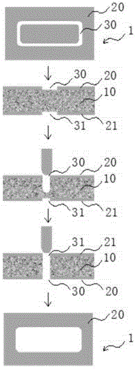
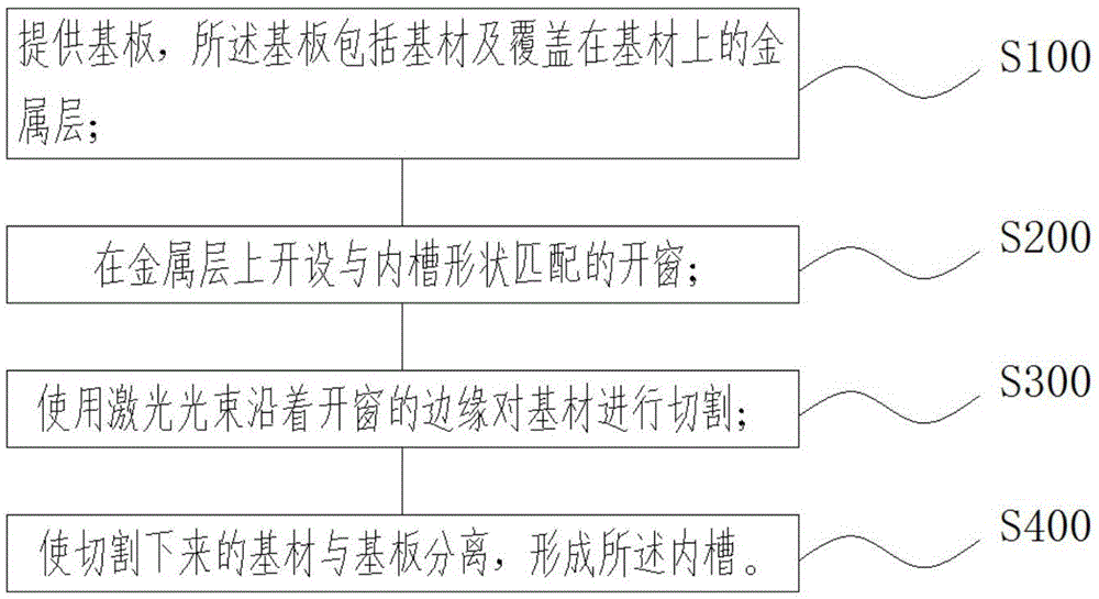
[0034] refer to figure 1 , 2 As shown, the processing method of the circuit board inner groove described in this embodiment comprises the following steps:

[0035] S100: providing a substrate 1, the substrate 1 comprising a base material 10 and a metal layer covering the base material 10;

[0036] In this embodiment, the substrate 1 includes a substrate 10 , a first metal layer 20 covering the first surface of the substrate 10 , and a second metal layer 21 covering the second surface of the substrate 10 . In this embodiment, a copper clad laminate is used as the substrate 1 .

[0037] S200: opening windows matching the shape of the inner tank on the metal layer;

[0038] Specifically, a first window 30 matching the shape of the inner groove is opened on the first metal layer 20 , and a second window 31 is opened on the second metal layer 21 at a position corresponding to the first window 30 . Pre...


PUM

PropertyMeasurementUnit
Spot diameteraaaaaaaaaa

Abstract

The invention discloses a circuit board inner groove machining method. The circuit board inner groove machining method comprises the following steps of providing a substrate, wherein the substrate comprises a base material and a metal layer covering the base material; forming an open window matched with the shape of the inner groove in the metal layer; cutting the base material by a laser beam along the edge of the open window; and enabling the cut base material to be separated from the base plate to form the inner groove. According to the circuit board inner groove machining method, the base material is continuously burnt and etched by a thermal effect of laser so as to fulfill the purpose of cutting; the metal layer is relatively low in laser absorption efficiency and relatively high in melting point, and the required destroy energy is relatively high, so that the metal layer is hard to machine by laser; therefore, the open window is formed in the metal layer before performing laser cutting, so that laser only acts on the base material; the laser beam cuts the base material along the edge of the open window, and point machining is converted into continuous processing, so that the circular bead machining limitation for an ultra-small circular bead inner groove is eliminated; and meanwhile, the machining efficiency and the machining precision are effectively improved.

Description

technical field [0001] The invention relates to the technical field of circuit board manufacturing, in particular to a method for processing inner grooves of a circuit board. Background technique [0002] With the development of electronic products in the direction of thinner and smaller, the requirements for the integration of circuit boards as carriers of electronic products are also getting higher and higher. In order to realize the miniaturization of the overall assembly volume of some products, different types of inner grooves are designed on the circuit board, which facilitates the installation of components and reduces the installation space. It includes a design of an ultra-small rounded inner groove. The main feature of the rounded inner groove is that the corners are rounded, the radius of the rounded corner is R≤0.30mm, and the length and width of the groove are ≤2.0mm. [0003] For the production of the above ultra-small rounded inner grooves, the conventional p...

Claims


Application Information

Patent Timeline
IPC IPC(8): H05K3/00
CPCH05K3/0044H05K2203/0228
Inventor 谢添华孙宏超王名浩
Owner GUANGZHOU FASTPRINT CIRCUIT TECH
Why Eureka
Try Eureka