Technology Mapping Method of Adder with Optimum Layout Structure Based on FPGA

A technology of process mapping and layout structure, which is applied in the fields of instrumentation, calculation, electrical digital data processing, etc., can solve problems such as inability to use adders to calculate, and achieve the effect of optimizing chip layout structure

Active Publication Date: 2019-04-09
CAPITAL MICROELECTRONICS
View PDF5 Cites 0 Cited by
  • Summary
  • Abstract
  • Description
  • Claims
  • Application Information

AI Technical Summary

Problems solved by technology

But in some cases, the current adder may only occupy a small part of the LUT4C resources in the next LE, and the rest of the free LUT4C resources cannot be used for another adder's operation due to the limitation of the carry input.

Method used


Image

  • Technology Mapping Method of Adder with Optimum Layout Structure Based on FPGA
  • Technology Mapping Method of Adder with Optimum Layout Structure Based on FPGA
  • Technology Mapping Method of Adder with Optimum Layout Structure Based on FPGA

Examples


Embodiment 1

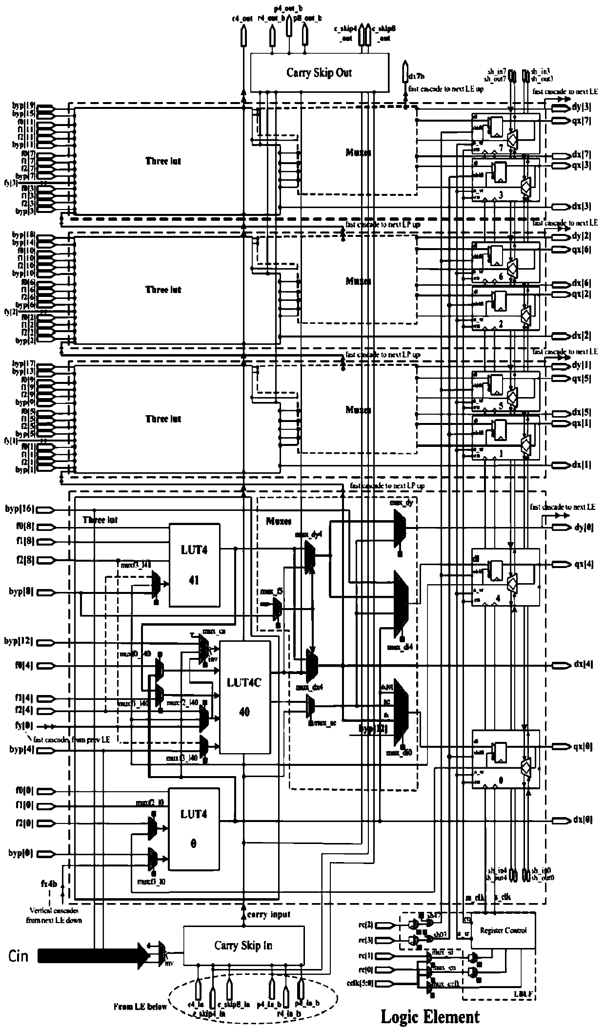
[0028] In this embodiment, a process mapping method of an n-bit full adder with an optimized layout structure is taken as an example for illustration. Logic diagram such as image 3 shown.

[0029] The addition logical operation of the present embodiment is: calculate the sum s (n bits) of the first addend a of n bits and the second addend b of n bits, wherein the carry input signal of the lowest bit of the addition is ci, and the addition operation The carry out signal is co. n is an integer and not less than 1.

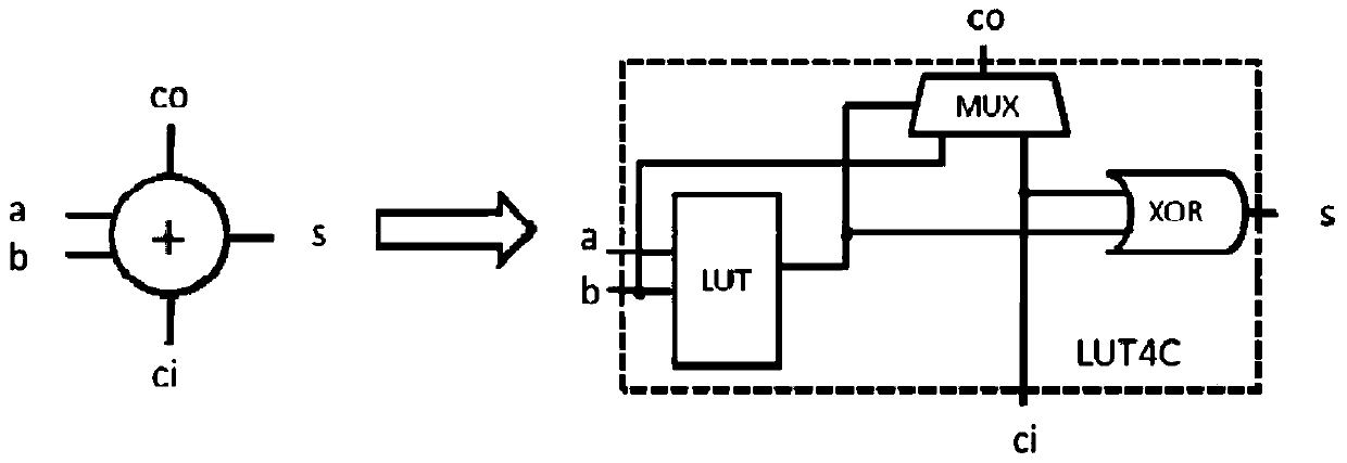
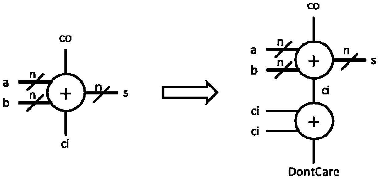
[0030] In this embodiment, the carry input ci is realized by the logic operation of a single one-bit adder. Specifically:

[0031] The two input terminals of an adder (implemented by LUT4C) respectively input the carry input signal ci of the lowest bit of the addition, that is, the logic for calculating ci+ci. When ci=0, no matter the carry input signal of the adder is 1 or 0, its carry output signal is 0; when ci=1, no matter the carry input signal of the adde...

Embodiment 2

[0037] In this embodiment, a process mapping method in which an m-bit full adder with an optimized layout structure and an n-bit full adder are cascaded through a LUT4C is taken as an example for illustration. Logical map such as Figure 5 shown.

[0038] Wherein, the addition logic operation of the n-bit full adder is: calculate the sum sa (n-bit) of the first addend a of n-bit and the second addend b of n-bit, wherein the carry input signal of the lowest bit of addition is cia , the carry output signal of the addition operation is coa. n is an integer and not less than 1.

[0039] The addition logic operation of the m-bit full adder is: calculate the sum sb (m-bit) of the first addend c of m-bit and the second addend d of m-bit, wherein the carry input signal of the lowest bit of the addition is cib, and the addition The carry output signal of the operation is cob. m is an integer and not less than 1.

[0040] The process mapping method provided by the above embodiments...


PUM


Abstract

The invention relates to an FPGA-based summator technology mapping method for optimizing a layout structure. The method comprises the following steps: inputting a carry input signal of a first summator at each of two input ends of an LUT4C with a carry chain in one logic portion (LP) of one logical element (LE) of the FPGA; carrying out an logical operation on the two input carry input signals by the LUT4C and then outputting a sum and a first carry output signal; and connecting the first carry output signal to a carry input end of the first summator. Through using one LUT4C to generate a carry input signal of the lowest order, the starting position of the carry chain is not restricted by FPGA architecture any longer and can lie in any carry element of the LE, thus optimizing the layout structure and size of a chip.

Description

technical field [0001] The invention relates to the technical field of integrated circuits, in particular to a process mapping method for an adder based on an FPGA-optimized layout structure. Background technique [0002] Field Programmable Gate Array (Field-Programmable Gate Array, FPGA) is a logic device with abundant hardware resources, powerful parallel processing capability and flexible reconfigurable capability. These features make FPGA more and more widely used in data processing, communication, network and many other fields. [0003] Addition is the most commonly used logic structure. The reason why FPGA has an arithmetic logic structure is mainly to optimize the speed and implementation of addition. Inside an FPGA, an adder is usually implemented by a carry chain. However, due to the limitations of the FPGA architecture, the lowest bit carry of an n-bit full adder can usually only be entered from the bottom dedicated carry input in the logic unit (Logic Element, L...

Claims


Application Information

Patent Timeline
Patent Type & Authority Patents(China)
IPC IPC(8): G06F17/50
Inventor 耿嘉刘明
Owner CAPITAL MICROELECTRONICS
Why Eureka
Try Eureka