Three-dimensional reconstruction method for image of scanning electron microscope

A technology of scanning electron microscopy and three-dimensional reconstruction, which is applied in image data processing, instrumentation, calculation, etc., can solve the problems of SEM imaging brightness and surface topography relationship expression error, SEM image is particularly sensitive, etc., to shorten the manufacturing or R&D cycle, avoiding physical damage, and improving product yield

Active Publication Date: 2016-05-18
北京中科微投资管理有限责任公司
View PDF5 Cites 14 Cited by
  • Summary
  • Abstract
  • Description
  • Claims
  • Application Information

AI Technical Summary

Problems solved by technology

However, this method has many shortcomings, such as the SFS algorithm is accompanied by a huge amount of calculation and calculation time; the SFS algorithm is particularly sensitive to SEM images with noise; the deviation between various assumptions and reality in the process of solving ill-conditioned equations; The surface topography relationship expression has a larg

Method used


Image

  • Three-dimensional reconstruction method for image of scanning electron microscope
  • Three-dimensional reconstruction method for image of scanning electron microscope
  • Three-dimensional reconstruction method for image of scanning electron microscope

Examples


Embodiment Construction

[0016] Embodiments of the present invention will be described in detail below with reference to the accompanying drawings, examples of which are shown in the drawings, wherein the same or similar reference numerals represent the same or similar elements or elements having the same or similar functions throughout. The embodiments described below by referring to the figures are exemplary only for explaining the present invention and should not be construed as limiting the present invention.

[0017] Furthermore, the present invention may repeat reference numerals and / or letters in different instances. This repetition is for the purpose of simplicity and clarity and does not in itself indicate a relationship between the various embodiments and / or arrangements discussed.

[0018] In order to better understand the technical solutions and technical effects of the present invention, a preferred embodiment of the present invention will be described in detail below in conjunction with ...


PUM


Abstract

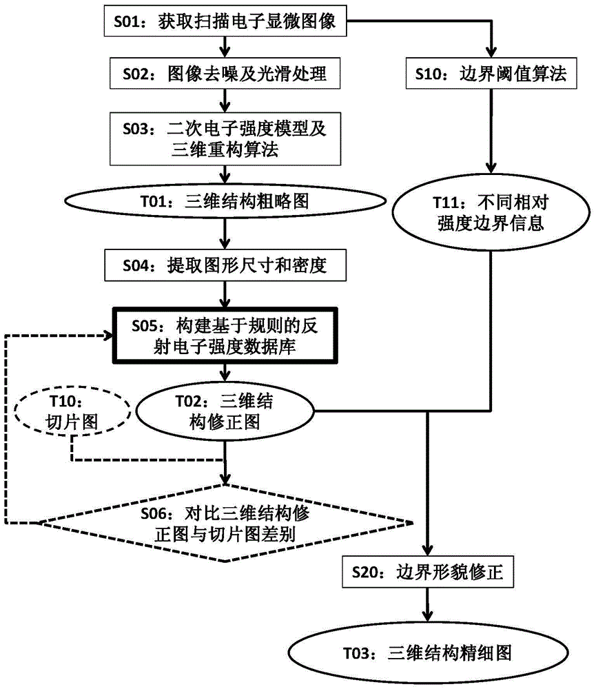
The invention provides a three-dimensional reconstruction method for the image of a scanning electron microscope. The method comprises the steps of providing a micro-nano structure; obtaining the image of a scanning electron microscope of the micro-nano structure; according to the image of the scanning electron microscope, obtaining a rough graph of a three-dimensional structure; according to the image of the scanning electron microscope, constructing a reflection electron intensity database; according to the reflection electron intensity database, correcting the rough graph of the three-dimensional structure to obtain a corrected graph of the three-dimensional structure; obtaining the boundary information of the micro-nano structure and correcting the corrected graph of the three-dimensional structure based on the boundary information so as to obtain the fine graph of the three-dimensional structure.

Description

technical field [0001] The invention relates to the field of semiconductors and scanning electronic imaging, in particular to the three-dimensional reconstruction technology of microscopic images viewed from above by micro-nano devices. Background technique [0002] Scanning Electronic Microscopy (SEM) technology plays a very important role in microscopic imaging of micro-nano devices. It is currently the most widely used micro-nano structure observation and measurement technology in the field of integrated circuits. It has high resolution and imaging speed Fast, less damage to the device structure and other advantages. The imaging of surface topography by SEM is mainly based on the secondary electrons generated by the inelastic scattering of electrons and atoms, which escape from the surface and are then collected by the detector. Since the secondary electrons can only escape from the range of 10nm below the surface, SEM can better reflect the surface topography and is cur...

Claims


Application Information

Patent Timeline
IPC IPC(8): G06T17/00
Inventor 张利斌粟雅娟韦亚一
Owner 北京中科微投资管理有限责任公司
Why Eureka
Try Eureka