LED light source substrate and manufacturing method thereof

A technology of LED light source and manufacturing method, which is applied in the direction of electrical components, circuits, semiconductor devices, etc., and can solve the problem of poor control of the quality of wire bonding and phosphor coating, affecting the packaging yield of LED light source, and prone to problems, etc. problems, to achieve the effects of avoiding capacity bottlenecks, saving gold wire consumables, and high product yields

Inactive Publication Date: 2016-05-18
泉州市金太阳照明科技有限公司
View PDF3 Cites 3 Cited by
  • Summary
  • Abstract
  • Description
  • Claims
  • Application Information

AI Technical Summary

Problems solved by technology

Different preparation methods have their own advantages and disadvantages, and the disadvantages mainly focus on the restrictions on the process during preparation
At present, in the LED white light manufacturing process, crystal bonding, wire bonding, powder application, baking, and testing are common process routes. In this manufacturing process, the quality of wire bonding and the quality of phosphor coating will affect the packaging quality of LED light sources. rate, but the quality of wire bonding and the quality of phosphor coating are not easy to control, and problems are prone to occur

Method used


Image

  • LED light source substrate and manufacturing method thereof
  • LED light source substrate and manufacturing method thereof
  • LED light source substrate and manufacturing method thereof

Examples


Embodiment Construction

[0018] In order to make the purpose, features and advantages of the present invention clearer, the specific implementation of the present invention will be described in more detail below in conjunction with the accompanying drawings and embodiments. In the following description, many specific details are set forth for the convenience of The invention is fully understood, but it can be practiced in many other ways than that described. Accordingly, the present invention is not limited to the specific implementations disclosed below.

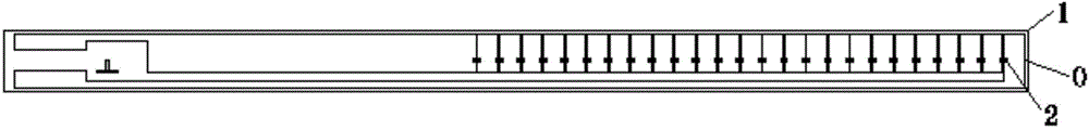
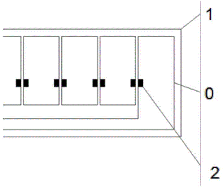
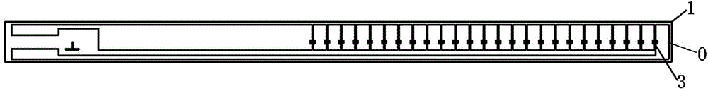
[0019] Such as Figure 1-Figure 6 Shown, a kind of manufacturing method of LED light source substrate, comprises the following steps:

[0020] S1, printing solder paste: such as figure 1 , figure 2 As shown, on the substrate 1 with the line 0 set, the solder paste 2 is printed on the positions corresponding to the positive and negative electrodes of the LED chip, and the solder paste 2 is printed by stencil printing;

[0021] S2, solid crystal...


PUM


Abstract

The invention discloses an LED light source substrate and a manufacturing method thereof. The method comprises: solder paste printing is carried out; to be specific, positions, corresponding to a positive electrode and a negative electrode of an LED chip, are printed with solder pastes on a substrate with a set circuit; die bonding is carried out; to be specific, the LED chip is pasted on the substrate, wherein the positive electrode position and the negative electrode position of the LED chip correspond to the positions, with the solder pastes, of the positive electrode and the negative electrode on the substrate; reflow soldering is carried out; to be specific, the substrate after the die bonding is sent into a hot-air reflow soldering furnace cavity and thus the substrate circuit and the LED chip are welded together by melting of the solder pastes; a phosphor glue layer is sprayed; to be specific, a phosphor glue layer is sprayed around the LED chip and is solidified by baking by an oven; and then a fluorescent film layer is pasted; to be specific, a fluorescent film is pasted on the surface of the phosphor glue layer and baking is carried out by the oven to enable the fluorescent film and the phosphor glue layer are in contact. Therefore, the routing process is reduced; and with spraying of the phosphor glue layer and pasting of the fluorescent film layer, the yield of the manufactured LED light source product is high and the light colors are uniform.

Description

technical field [0001] The invention relates to the technical field of LED lighting, in particular to an LED light source substrate and a manufacturing method thereof. Background technique [0002] Semiconductor light-emitting diodes (LEDs) have the advantages of low energy consumption and long service life. Under the background of energy-saving and carbon-reduction policies, they are the next-generation ideal light sources to replace incandescent lamps, energy-saving lamps and other lighting sources. With the continuous improvement of chip manufacturing capabilities, the luminous efficiency and brightness of light-emitting diodes continue to increase, and the cost performance of LED application products that use light-emitting diodes as lighting sources continues to rise. In the case of lighting, the energy saving effect of replacing traditional light source lamps with LEDs is obvious. [0003] At present, there are many ways to prepare white LED light sources. For exampl...

Claims


Application Information

Patent Timeline
Patent Type & Authority Applications(China)
IPC IPC(8): H01L33/00H01L33/50H01L33/48H01L33/62
Inventor 林朝晖邱新旺苏锦树
Owner 泉州市金太阳照明科技有限公司
Why Eureka
Try Eureka