Packaging structure of light-emitting diode

A technology of light-emitting diodes and packaging structures, which is applied to electrical components, electrical solid devices, circuits, etc., and can solve problems such as weak mechanical strength and easy breakage

Active Publication Date: 2016-05-18
ZHANJING TECH SHENZHEN +1
View PDF5 Cites 0 Cited by
  • Summary
  • Abstract
  • Description
  • Claims
  • Application Information

AI Technical Summary

Problems solved by technology

However, in the prior art, in order to meet the miniaturization and thinning design requirements of semiconductor components, the shell of the light emitting diode packaging structure is usually designed to be thinner, resulting in relatively weak mechanical strength and prone to breakage

Method used


Image

  • Packaging structure of light-emitting diode
  • Packaging structure of light-emitting diode
  • Packaging structure of light-emitting diode

Examples


Embodiment Construction

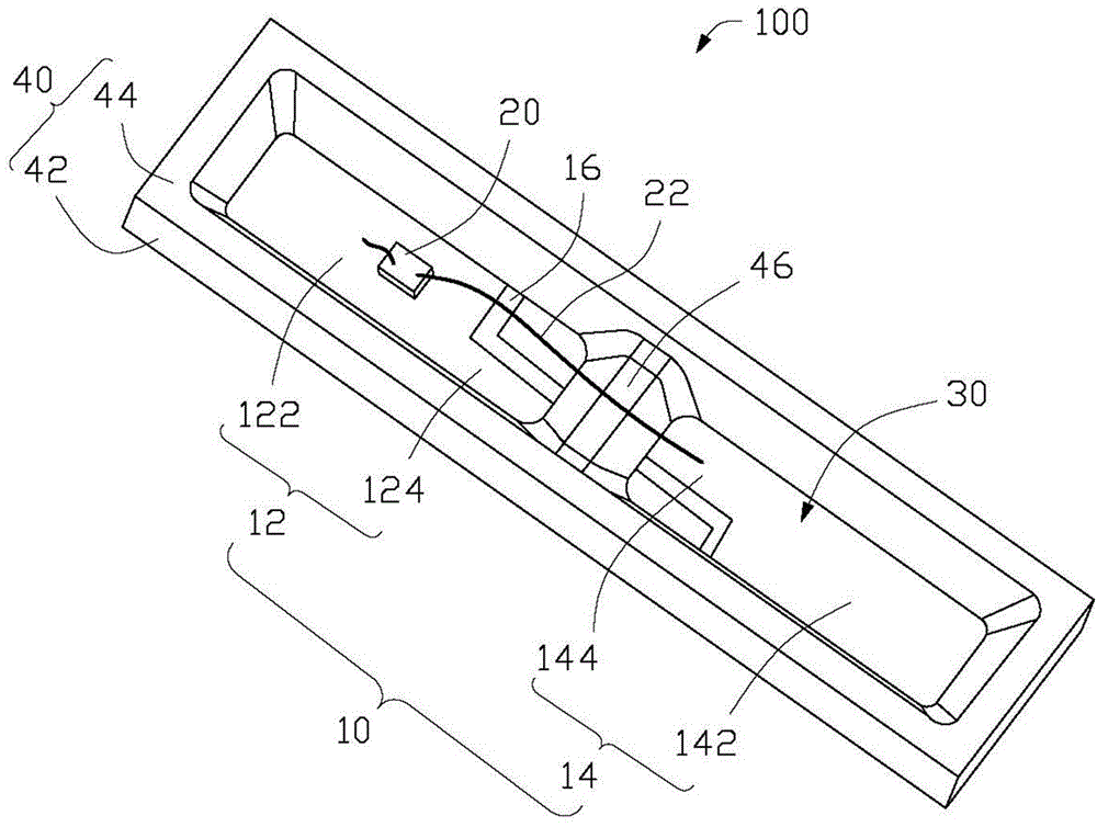
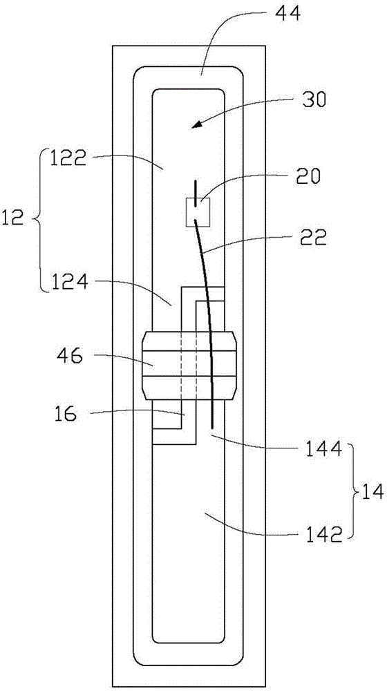
[0014] see Figure 1 to Figure 3 , the light emitting diode packaging structure 100 of the embodiment of the present invention, which includes at least two electrodes 10, at least one light emitting diode chip 20 electrically connected to the at least two electrodes 10, a package body 30 covering the light emitting diode chip, and the The package body 30 and the housing 40 surrounding the light-emitting diode chip 20 include a base 42 and a reflective cup 44 extending upward from the base 42. The reflective cup 44 connects the light-emitting diode Surrounding the chip 20 , the casing 40 further includes a support 46 , the support 46 is disposed inside the reflection cup 44 and straddles the at least two electrodes 10 .

[0015] The at least two electrodes 10 include a first electrode 12 and a second electrode 14 . The first electrodes 12 and the second electrodes 14 are arranged at intervals. The first electrode 12 includes a first body portion 122 and a first extension port...


PUM


Abstract

The invention relates to a packaging structure of a light-emitting diode. The packaging structure comprises at least two electrodes, at least one light-emitting diode chip connected with the at least two electrodes electrically, a packaging body covering the light-emitting diode chip, and a housing encircling the packaging body and the light-emitting diode chip. The housing includes a pedestal and a reflection cup extending upwardly from the pedestal; and the light-emitting diode chip is encircled by the reflection cup. Besides, the housing also includes a supporting element that is arranged inside the reflection cup and stretches across the at least two electrodes.

Description

technical field [0001] The invention relates to a semiconductor element, in particular to a light emitting diode packaging structure. Background technique [0002] Compared with traditional light sources, Light Emitting Diode (LED) has the advantages of light weight, small size, low pollution, long life, etc. As a new type of light source, it has been increasingly used in various fields Among them, such as street lights, traffic lights, signal lights, spotlights and decorative lights. [0003] Existing LED packaging structures generally include electrodes, LED chips electrically connected to the electrodes, a packaging body covering the LED chips on a substrate, and a casing surrounding the aforementioned structure and playing a supporting role. However, in the prior art, in order to meet the miniaturization and thinning design requirements of the semiconductor element, the shell of the light emitting diode packaging structure is usually designed to be thinner, resulting in...

Claims


Application Information

Patent Timeline
Patent Type & Authority Applications(China)
IPC IPC(8): H01L33/48H01L33/60
CPCH01L33/60H01L33/486H01L33/62H01L2224/48247H01L2224/48257
Inventor 林厚德张超雄陈滨全陈隆欣
Owner ZHANJING TECH SHENZHEN
Why Eureka
Try Eureka