Check patentability & draft patents in minutes with Patsnap Eureka AI!

Array package-based FPGA (field programmable gate array) chip

An array packaging and chip technology, applied in special data processing applications, instruments, electrical digital data processing, etc., can solve the difficulty of placing the filter capacitor of the I/O power supply, the irregular arrangement of the outermost pins of the FPGA chip, and the I /O fan-out problems and other issues, to achieve the effect of optimizing the peripheral pin layout, good effect, and easy placement

Active Publication Date: 2016-05-25
SHENZHEN PANGO MICROSYST CO LTD
View PDF3 Cites 2 Cited by
  • Summary
  • Abstract
  • Description
  • Claims
  • Application Information

AI Technical Summary

Problems solved by technology

[0004] The outermost pin arrangement of the traditional BGA-packaged FPGA chip is irregular, and the influence of the arrangement of the pads on the fan-out of the I / O and the layout of the filter capacitor of the I / O power supply during PCB board-level design is not fully considered. , often resulting in difficulty in I / O fan-out in PCB board-level design or the need to increase the number of PCB layers to fan out all I / O, and the placement of filter capacitors for I / O power supplies is also difficult

Method used


Image

  • Array package-based FPGA (field programmable gate array) chip
  • Array package-based FPGA (field programmable gate array) chip
  • Array package-based FPGA (field programmable gate array) chip

Examples


Embodiment Construction

[0019] In order to make the purpose, technical solutions and advantages of the embodiments of the present invention clearer, the technical solutions in the embodiments of the present invention will be clearly and completely described below in conjunction with the drawings in the embodiments of the present invention. Obviously, the described embodiments It is only some embodiments of the present invention, but not all embodiments. Based on the embodiments of the present invention, all other embodiments obtained by persons of ordinary skill in the art without making creative efforts belong to the protection scope of the present invention.

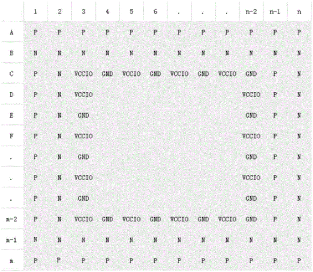
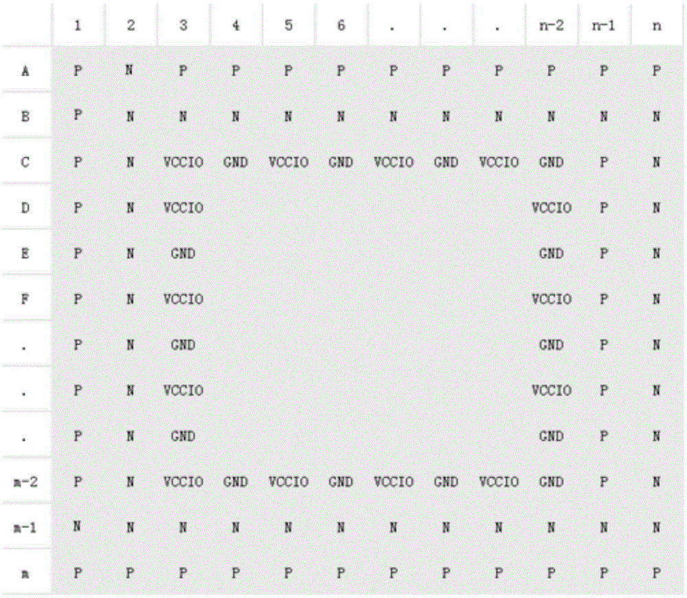
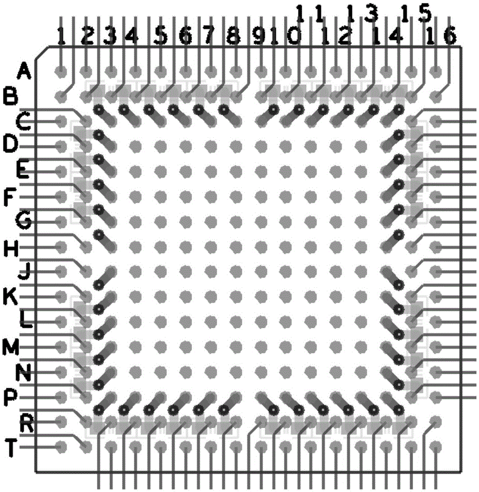
[0020] The present invention provides a FPGA chip based on array packaging, as attached figure 1 As shown, the outermost two circles of pins of the FPGA chip are I / O pins, the outermost row of I / O pins and the second outer row of I / O pins form a differential pair in the vertical direction, and the outermost row of I / O pins and the second out...


PUM


Abstract

The invention provides an array package-based FPGA (field programmable gate array) chip. Outermost two circles of pins of the FPGA chip are I / O (input / output) pins, an outermost row of the I / O pins and a secondarily outermost row of I / O pins form differential pairs in a longitudinal direction, and an outermost column of the I / O pins and a secondarily outermost column of the I / O pins form differential pairs in a transverse direction. The invention enables easier I / O fan-out and reduces the quantity of PCB (printed circuit board) design layers; meanwhile, a filter capacitor of an I / O power supply is easier and more reasonable to place, with better filtration effect.

Description

technical field [0001] The invention relates to the technical field of integrated circuit design, in particular to an FPGA chip based on array packaging. Background technique [0002] FPGA (Field Programmable Gate Array, Field Programmable Gate Array), as a semi-custom circuit in the field of application-specific integrated circuits, not only solves the shortcomings of custom circuits, but also overcomes the shortcomings of the limited number of original programmable device gates. With the development of FPGA technology, the number of I / Os continues to increase. At present, most FPGA chips are packaged in BGA (BallGridArray, solder ball array package). The number of pins in this package ranges from dozens to as many as More than a thousand, and most of the I / O can be used in differential pairs. The FPGA chip generally has several groups (BANK), and the voltage value of the I / O power supply of each group is the same. To obtain better signal integrity on the I / O, the I / O powe...

Claims


Application Information

Patent Timeline
Patent Type & Authority Applications(China)
IPC IPC(8): G06F17/50H01L27/02
CPCG06F30/392H01L27/0203
Inventor 张亚林
Owner SHENZHEN PANGO MICROSYST CO LTD
Features
  • R&D
  • Intellectual Property
  • Life Sciences
  • Materials
  • Tech Scout
  • Unparalleled Data Quality
  • Higher Quality Content
  • 60% Fewer Hallucinations
Learn More