Improved waveguide probe transition based structure for performing modular packaging for chip

A modular, probe technology, applied in the direction of semiconductor devices, semiconductor/solid-state device parts, electrical components, etc., can solve the problems of chip energy transmission limitation, poor matching of module input and output ports, etc., to achieve good return loss, The effect of low insertion loss and easy processing

Inactive Publication Date: 2016-05-25
INST OF ELECTRONICS ENG CHINA ACAD OF ENG PHYSICS
View PDF12 Cites 7 Cited by
  • Summary
  • Abstract
  • Description
  • Claims
  • Application Information

AI Technical Summary

Problems solved by technology

[0003] The modular packaging of chips in the millimeter wave and terahertz frequency bands requires gold wire bonding, which will introduce additional losses, and will deteriorate the matching of the chip's module input and output ports, limiting the energy transmission of the chip

Method used


Image

  • Improved waveguide probe transition based structure for performing modular packaging for chip
  • Improved waveguide probe transition based structure for performing modular packaging for chip
  • Improved waveguide probe transition based structure for performing modular packaging for chip

Examples


Embodiment

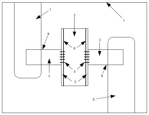
[0026] Such as Figure 1~3 As shown, the chip is modularly packaged based on the improved waveguide probe transition structure, including a metal cavity 1; the metal cavity is provided with more than one waveguide cavity, and more than one transition probe 2; the transition One end of the probe is located in the waveguide cavity, and the other end of the transition probe is provided with a chip 3 that needs to be packaged; the chip is connected to the transition probe through a bonding gold wire 4, and a conductive glue is provided at the junction 5 or / and metal boss 6.

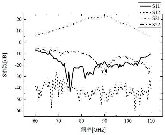
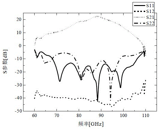
[0027] Among them, the metal cavity can be gold-plated for good grounding; the probe adopts a multi-level high and low impedance matching section structure to achieve a good match between the chip and the module port; The section where the chip connects with the transition probe is edge-sealed with conductive glue, which significantly reduces the loss caused by the modular package. As a preference, the chip...


PUM


Abstract

The invention discloses an improved waveguide probe transition based structure for performing modular packaging for a chip. The improved waveguide probe transition based structure comprises a metal cavity; more than one waveguide cavity and more than one transition probe are arranged in the metal cavity; one end of each transition probe is positioned in the waveguide cavity while the other end of the transition probe is provided with the chip needing to be packaged; the chip is connected with the corresponding transition probe through a bonding gold thread, and conductive adhesive or/and a metal lug boss is arranged in the junction between the chip and the transition probe. The improved waveguide probe transition based structure is low in return loss, so that the energy reflection between a packaging module and the chip is effectively reduced.

Description

technical field [0001] The invention relates to the technical fields of microwave, millimeter wave and terahertz communication, in particular to a structure for modular packaging of chips based on an improved waveguide probe transition. Background technique [0002] With the rapid development of integrated circuit technology, the operating frequency of chips has entered the millimeter wave and terahertz frequency bands, and has the advantages of high integration and low cost. Great progress has been made in integrated transceiver circuits and integrated unit circuits. [0003] The modular packaging of the chip in the millimeter wave and terahertz frequency bands requires the use of gold wire bonding, which will introduce additional losses, and will make the matching of the module input and output ports of the chip worse, so that the energy transmission of the chip is limited. [0004] The waveguide cavity can transmit energy with low loss in a wide bandwidth, and the quartz ...

Claims


Application Information

Patent Timeline
Patent Type & Authority Applications(China)
IPC IPC(8): H01L23/66
CPCH01L23/66
Inventor 王瑞涛唐海林熊永忠
Owner INST OF ELECTRONICS ENG CHINA ACAD OF ENG PHYSICS
Why Eureka
Try Eureka