Optical microscope based on surface plasma resonance
A technology of surface plasmon and optical microscopy, which is applied in the direction of material analysis, scientific instruments, and measuring devices through optical means. The effect of sensitivity
- Summary
- Abstract
- Description
- Claims
- Application Information
AI Technical Summary
Problems solved by technology
Method used
Image
Examples
Embodiment Construction
[0030] The present invention is specifically described below by the embodiment, only for further illustrating the present invention, can not be interpreted as the limitation of protection scope of the present invention, the technical engineer of this field can make some non-essential improvements and improvements to the present invention according to the content of the above-mentioned invention Adjustment.
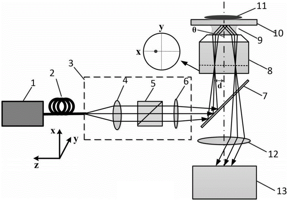
[0031] refer to figure 1 The schematic diagram of the structure shown, in accordance with the order of the optical path, each component is a laser generator 1, an optical fiber 2, a mobile platform 3, a collimator lens 4, a polarizer 5, a condenser lens 6, a beam splitter 7, and an optical microscope magnifying objective lens 8, Matching oil 9, plasmon resonance sensor chip 10, sample to be tested 11, lens 12, image sensor 13.
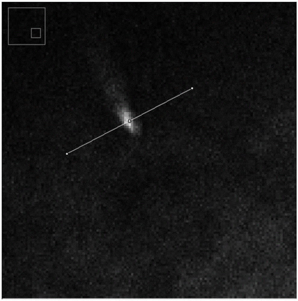
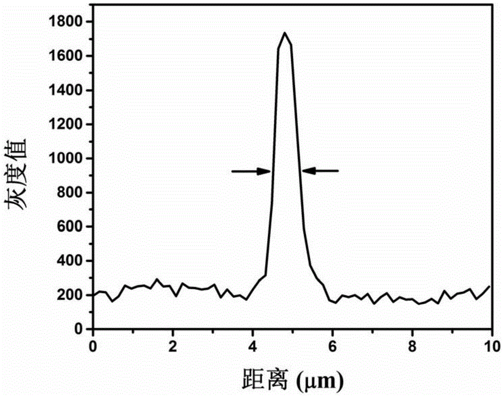
[0032] Take the detection of a gold nanoparticle with a diameter of 80nm by SPR microscope as an example to illustrate the experimental steps of ...
PUM
| Property | Measurement | Unit |
|---|---|---|
| Thickness | aaaaa | aaaaa |
Abstract
Description
Claims
Application Information


