
A kind of output circuit of SRAM

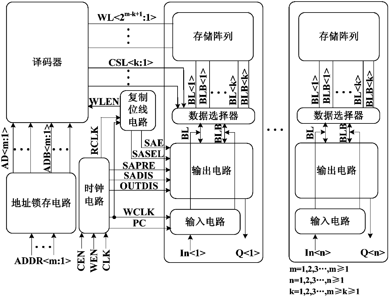
A static random, output circuit technology, applied in the field of output circuits, can solve the problems of reading data power consumption difference, static random access memory differential power consumption analysis attack threat, not suitable for design defense power consumption attack static random access memory and other problems, to eliminate Effects of Inconsistent Wiring Capacitance

Active Publication Date: 2018-03-23
NINGBO UNIV
View PDF1 Cites 0 Cited by
  • Summary
  • Abstract
  • Description
  • Claims
  • Application Information

AI Technical Summary

Problems solved by technology

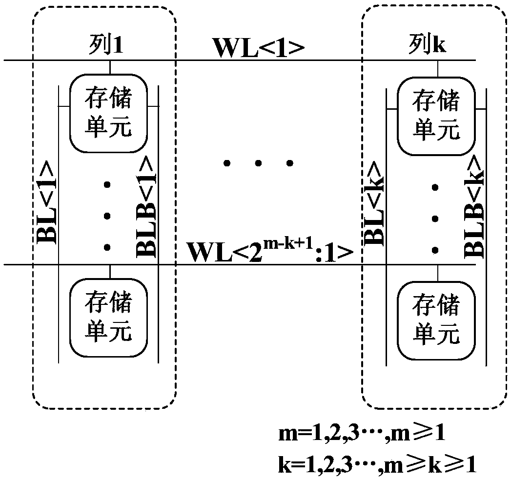
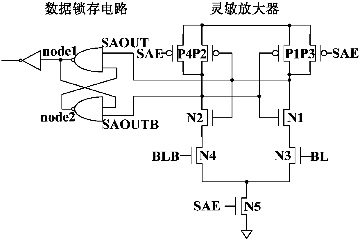
[0007] In the read-in phase, the sense amplifier output nodes SAOUT and SAOUTB maintain a high level state, the data latch circuit maintains the original output data, and then opens the pull-down path in the evaluation phase, and the voltage difference between the bit line pair BL and BLB causes the NMOS transistor N3 Different from the pull-down current of the NMOS transistor N4, under the positive feedback of the two mutually coupled inverters of the sense amplifier, the voltage difference between the output nodes SAOUT and SAOUTB is quickly formed, but the wiring capacitance caused by process deviation and unbalanced wiring is inconsistent It will cause a certain difference in power consumption. At the same time, the data latch circuit determines whether the nodes node1 and node2 are flipped or held according to whether the data read in the current cycle is the same as the data read in the previous cycle, and the output terminal Q may be held, charged and Discharging three operations, causing the difference in power consumption associated with reading data
The supply current diagram of the output circuit in the existing SRAM under four different working states is as follows: Figure 5 shown, analysis Figure 5 It can be seen that the current difference in the evaluation stage is very obvious under different conditions, making the SRAM vulnerable to the threat of differential power analysis attack
[0008] For the existing SRAM, its output circuit is a single-ended output, because there is no completely consistent complementary output, so the dual-rail precharge logic is not suitable for use in the design of the SRAM, and the three-phase dual-rail precharge logic and The self-timed three-phase dual-rail precharge logic increases the discharge process on the basis of SABL, so that the main nodes in each cycle circuit can be charged and discharged once, and overcome the shortcomings of power consumption differences caused by inconsistent load and wiring capacitance, but due to their It is necessary to reset the output before the end of the cycle, and the read data cannot be maintained, so it is not suitable for designing SRAMs that defend against power consumption attacks

Method used


Image

  • A kind of output circuit of SRAM
  • A kind of output circuit of SRAM
  • A kind of output circuit of SRAM

Examples


Embodiment

[0024] Example: such as Figure 6 As shown, an output circuit of an SRAM includes a sense amplifier and a data latch circuit, and the sense amplifier includes a first PMOS transistor P1, a second PMOS transistor P2, a third PMOS transistor P3, a fourth PMOS transistor P4, and a fifth PMOS transistor P4. PMOS transistor P5, sixth PMOS transistor P6, seventh PMOS transistor P7, first NMOS transistor N1, second NMOS transistor N2, third NMOS transistor N3, fourth NMOS transistor N4 and fifth NMOS transistor N5; the first PMOS transistor The source of P1, the source of the fourth PMOS transistor P4 and the source of the fifth PMOS transistor P5 are connected to the power supply, the drain of the first PMOS transistor P1, the source of the second PMOS transistor P2 and the third PMOS transistor P3 The source of the second PMOS transistor P2, the gate of the third PMOS transistor P3, the drain of the fourth PMOS transistor P4, the drain of the sixth PMOS transistor P6, the drain of ...


PUM


Abstract

The invention discloses an output circuit of a static random access memory.The output circuit comprises a sense amplifier and a data latching circuit; the sense amplifier is composed of a first PMOS transistor, a second PMOS transistor, a third PMOS transistor, a fourth PMOS transistor, a fifth PMOS transistor, a sixth PMOS transistor, a seventh PMOS transistor, a first NMOS transistor, a second NMOS transistor, a third NMOS transistor, a fourth NMOS transistor and a fifth NMOS transistor, and the data latching circuit is composed of two NOR gates, an eighth PMOS transistor, a ninth PMOS transistor, a tenth PMOS transistor, an eleventh PMOS transistor, a sixth NMOS transistor, a seventh NMOS transistor, an eighth NMOS transistor, a ninth NMOS transistor and a tenth NMOS transistor.The output circuit has the advantages that the power consumption of all working periods keeps basically consistent when the static random access memory reads data, and the defense differential power analysis capacity of the static random access memory is improved.

Description

technical field [0001] The invention relates to an output circuit, in particular to an output circuit of a static random access memory. Background technique [0002] With the development of network technology and wireless communication technology, the security of personal information storage and transmission has received more and more attention. Electronic devices that store personal information usually ensure the security of information through encryption, but attackers can use side-channel attacks to obtain keys by using information such as power consumption, time, and electromagnetic waves leaked during hardware encryption. Differential power analysis is currently the most widely used and effective side-channel attack method. It obtains keys by analyzing the correlation between data processing and power consumption during hardware encryption, which seriously threatens the security of encryption devices. In recent years, scholars have found that eliminating the power cons...

Claims


Application Information

Patent Timeline
Patent Type & Authority Patents(China)
IPC IPC(8): G11C11/419
CPCG11C11/419
Inventor 汪鹏君周可基陈伟伟张跃军
Owner NINGBO UNIV
Learn More