A method for high and low temperature controllable wafer bonding using a semiconductor refrigeration chip

A wafer bonding and cooling chip technology, which is applied in semiconductor/solid-state device manufacturing, electrical components, circuits, etc., and can solve the problems of large wafer surface gap, difficulty in improving the annealing process, and unbonded wafers.

Active Publication Date: 2018-03-06
HARBIN INST OF TECH
View PDF2 Cites 0 Cited by
  • Summary
  • Abstract
  • Description
  • Claims
  • Application Information

AI Technical Summary

Problems solved by technology

Since the wafer itself has a certain warpage (~10 microns), the pre-bonding process is often due to insufficient water molecule adsorption on the wafer surface, and the gap between the warped wafer surfaces is too large (beyond the effect of van der Waals force or hydrogen bond) range), which resulted in pre-bonded wafers with large areas of unbonded areas and defects
These problems are difficult to improve only by subsequent annealing process

Method used


Image

  • A method for high and low temperature controllable wafer bonding using a semiconductor refrigeration chip
  • A method for high and low temperature controllable wafer bonding using a semiconductor refrigeration chip
  • A method for high and low temperature controllable wafer bonding using a semiconductor refrigeration chip

Examples


Embodiment Construction

[0032] The technical solution of the present invention will be further described below in conjunction with the accompanying drawings, but it is not limited thereto. Any modification or equivalent replacement of the technical solution of the present invention without departing from the spirit and scope of the technical solution of the present invention should be covered by the present invention. within the scope of protection.

[0033] The invention provides a method for high and low temperature controllable wafer bonding using a semiconductor refrigeration chip, and the specific implementation steps are as follows:

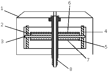
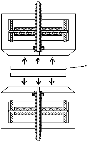
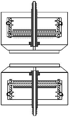
[0034] (1) Materials:

[0035] Prepare the first wafer, the second wafer, the first wafer indenter, the second wafer indenter, semiconductor cooling chip, thermal conductive silicone grease and experimental supplies related to activation treatment required for the experiment.

[0036] (2) Coating thermal grease:

[0037] The upper and lower surfaces of the semic...


PUM


Abstract

The invention provides a high and low temperature controllable wafer bonding method through a semiconductor refrigeration sheet. The method comprises the steps that a wafer is fit on a wafer pressing head; the cold surface of the semiconductor refrigeration sheet is fit with the wafer pressing head for cooling the wafer; bonding is performed under the pressure effect of the pressing head; the hot surface of the semiconductor refrigeration sheet is fit with the wafer pressing head for heating the wafer; and annealing is performed. The bonding process of the wafer is intervened through the cold surface of the semiconductor refrigeration sheet, temperature of the wafer is reduced by the mode of heat conduction and gas near the surface of the wafer is enabled to be liquefied, and then R-OH of original holes is connected through the bridging effect of water molecules under the effect of dual factors of certain external force and the water molecules so that formation of wafer pre-bonding holes can be reduced and even eliminated; besides, temperature of the bonded wafer is increased by the mode of heat conduction through the hot surface of the semiconductor refrigeration sheet so that annealing is completed under certain temperature, and thus the objectives of further reducing the number of the holes and increasing strength of a wafer bonding interface can be achieved.

Description

technical field [0001] The invention belongs to the field of semiconductor manufacturing, and relates to a method for bonding high and low temperature controllable wafers by using a semiconductor refrigerating sheet. Background technique [0002] In recent years, while the manufacturing industry is pursuing high performance devices, the integration of multifunctional electronic / optical / biomedical devices has also become one of the key driving forces for new electronic products. Joining (also known as "bonding") technology is an irreplaceable and important link in the integration of diverse and complex systems. With the continuous advancement of semiconductor process technology, the manufacturing industry is developing in the direction of high-volume and low-cost. Because direct bonding of large-area wafers can simplify the device manufacturing process and reduce production costs, it has increasingly attracted the attention of the industry. [0003] The traditional wafer bon...

Claims


Application Information

Patent Timeline
Patent Type & Authority Patents(China)
IPC IPC(8): H01L21/18H01L21/324
CPCH01L21/187H01L21/3247
Inventor 王晨曦许继开田艳红刘宝磊
Owner HARBIN INST OF TECH
Why Eureka
Try Eureka