High-power thyristor package structure and manufacturing method thereof

A manufacturing method and high-power technology, applied in semiconductor/solid-state device manufacturing, electrical components, electrical solid-state devices, etc., can solve the problems of device product performance decline, low production efficiency, large thermal conduction distance of devices, etc., and reduce thermal conduction distance. , Product performance improvement, the effect of improving the heat dissipation effect

Inactive Publication Date: 2016-06-01
JIANGSU JIEJIE MICROELECTRONICS
View PDF6 Cites 3 Cited by
  • Summary
  • Abstract
  • Description
  • Claims
  • Application Information

AI Technical Summary

Problems solved by technology

Since the front of the chip is welded with copper sheets, the overcurrent capability of the device is enhanced; but the disadvantages are: 1) The internal heat conduction distance of the device is large, the thermal resistance is large, the heat dissipation performance of the device is poor, and the performance of the device product is reduced; The chip control electrode area is welded with copper lead sheet, which is difficult to operate and the production efficiency is low

Method used


Image

  • High-power thyristor package structure and manufacturing method thereof
  • High-power thyristor package structure and manufacturing method thereof
  • High-power thyristor package structure and manufacturing method thereof

Examples


Embodiment Construction

[0035] In order to deepen the understanding of the present invention, the present invention will be further described in detail below. This embodiment is only used to explain the present invention, and does not constitute a limitation to the protection scope of the present invention.

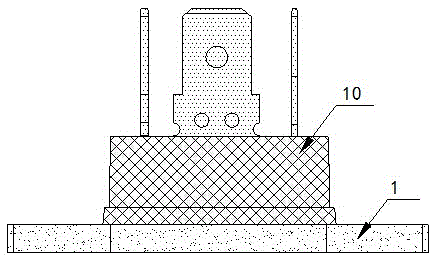
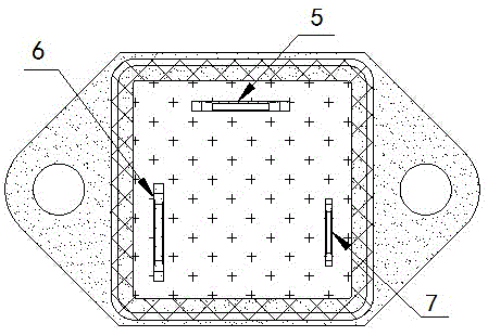
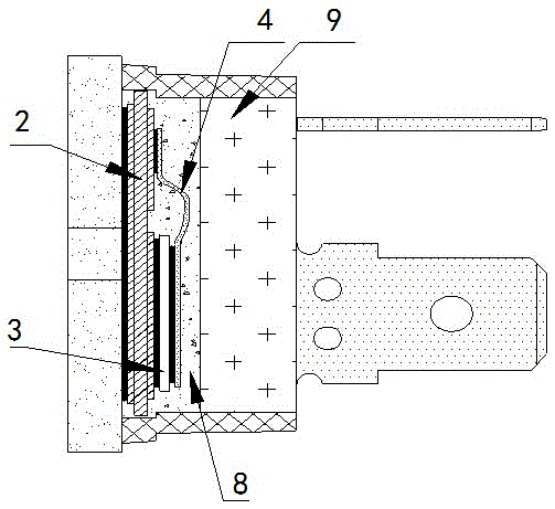
[0036] like Figure 1-4 As shown, a high-power thyristor packaging structure of the present invention includes a metal heat dissipation base plate 1 and a ceramic copper clad laminate 2 whose bottom surface is welded to the upper end of the metal heat dissipation base plate 1. The bottom surface of the ceramic copper clad plate 2 is a large-area copper clad layer. , Figure 6a , Figure 6b , Figure 6c As shown, the top surface of the ceramic copper clad laminate 2 is a copper clad layer divided into the anode welding zone 11, the cathode welding zone 12, and the gate electrode welding zone 13, and the upper end of the ceramic copper clad laminate 2 is sequentially welded with a thyristor chip...


PUM

PropertyMeasurementUnit
thicknessaaaaaaaaaa

Abstract

The invention discloses a high-power thyristor package structure, which comprises a metal cooling bottom plate and a ceramic copper-clad plate, wherein the bottom surface of the ceramic copper-clad plate is welded at the upper end of the metal cooling bottom plate; a large-area copper-clad layer is arranged on the bottom surface of the ceramic copper-clad plate; a copper-clad layer divided into an anode welding region, a cathode welding region and a gate welding region is arranged on the top surface of the ceramic copper-clad plate; a thyristor chip and an anode bridging chip are sequentially welded at the upper end of the copper-clad layer on the top surface of the ceramic copper-clad plate from bottom to top; a plastic sleeve shell is also arranged on the periphery of the ceramic copper-clad plate; and a cathode electrode and a gate electrode of the thyristor chip are welded on the divided cathode welding region and gate welding region on the top surface of the ceramic copper-clad plate in a coplanar inversion manner respectively. The invention further discloses a manufacturing method of the high-power thyristor package structure. By the method that the cathode electrode and the gate electrode of the thyristor chip are welded on the divided copper-clad layer on the top surface of the ceramic copper-clad plate in the coplanar inversion manner, the cooling effect is greatly improved; and meanwhile, the process of bridging assembly welding of a control electrode is emitted, so that massive high-efficiency production can be relatively well achieved.

Description

technical field [0001] The invention relates to a high-power thyristor packaging structure. [0002] The invention also relates to a manufacturing method of a high-power thyristor packaging structure. It belongs to the field of power semiconductor devices. Background technique [0003] One-way thyristors are widely used in AC non-contact switches, household appliances control circuits, industrial control and other fields. It is required to have strong heat dissipation capacity, low cost and high production efficiency. The one-way thyristors currently on the market are all packaged on the front with the gate and cathode, and the anode is welded to the heat dissipation bottom plate. The heat generated by the one-way thyristor mainly comes from the cathode area and the gate area. When the cathode area and the gate area are being welded, they are far away from the heat dissipation bottom plate, and the heat transfer is slow and the heat dissipation effect is poor. [0004] ...

Claims


Application Information

Patent Timeline
Patent Type & Authority Applications(China)
IPC IPC(8): H01L23/48H01L21/60
CPCH01L24/10H01L23/48H01L2224/40225H01L2224/0603
Inventor 吴家健王成森尹佳军
Owner JIANGSU JIEJIE MICROELECTRONICS
Why Eureka
Try Eureka