A super junction mosfet

A gate structure and substrate technology, applied in semiconductor devices, electrical components, circuits, etc., to improve the ability to resist UIS failures, suppress parasitic transistors from turning on, and improve reliability

Inactive Publication Date: 2019-03-29
UNIV OF ELECTRONICS SCI & TECH OF CHINA
View PDF4 Cites 0 Cited by
  • Summary
  • Abstract
  • Description
  • Claims
  • Application Information

AI Technical Summary

Problems solved by technology

UIS failure has gradually become one of the most important safety killers of power MOSFETs. Although traditional super-junction MOSFET devices have effectively solved the contradiction between breakdown voltage and on-resistance, they still have insufficient performance in terms of anti-UIS failure performance. there are many problems

Method used


Image

  • A super junction mosfet
  • A super junction mosfet
  • A super junction mosfet

Examples


Embodiment 1

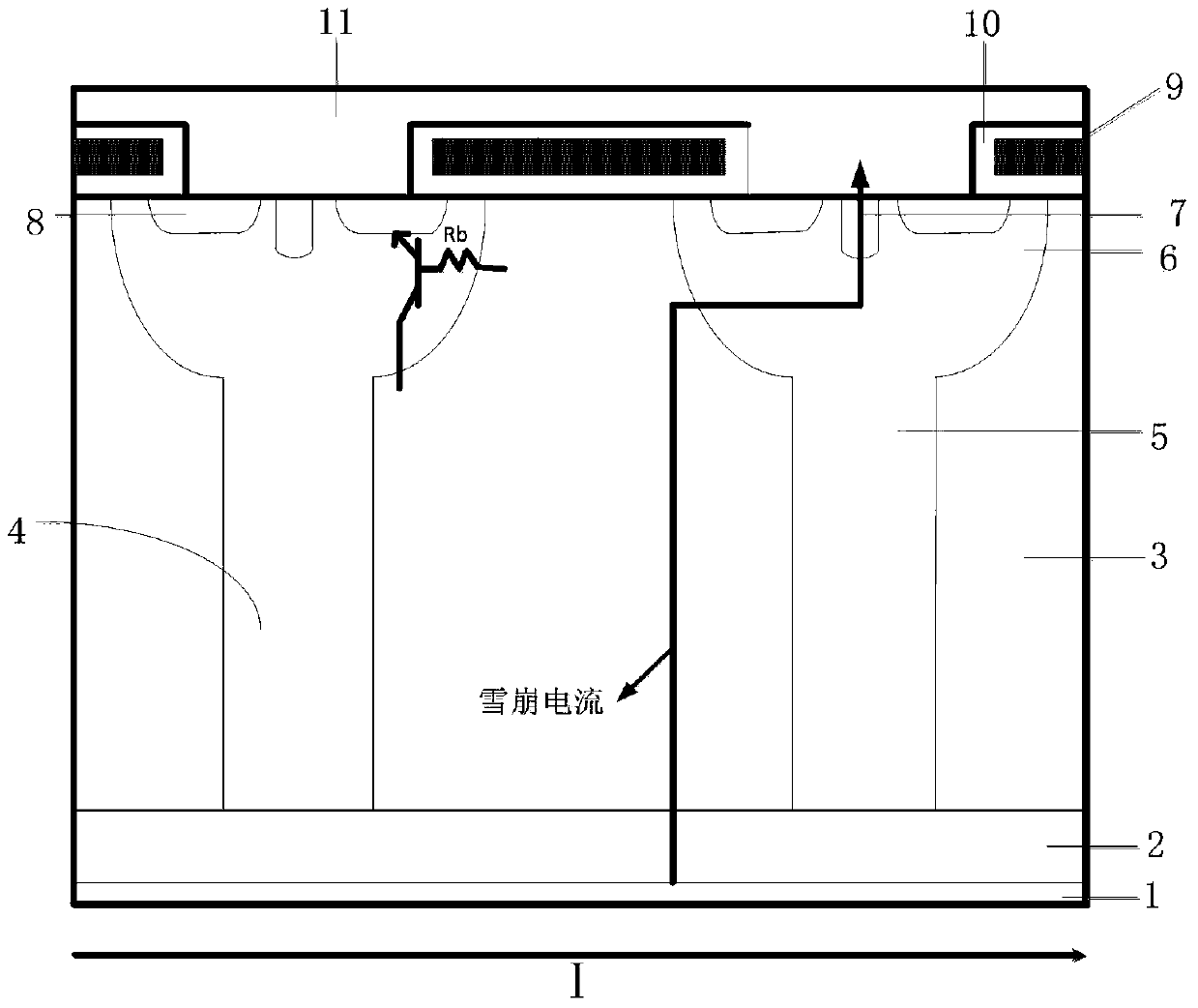
[0026] Such as figure 2 As shown, this example includes normal cell area I (only one cell is shown in the figure) and pseudo cell II; the normal cell area I and pseudo cell II share the same metal drain electrode 1, metal drain electrode 1 Above is the N+ substrate 2, and above the N+ substrate 2 is the N epitaxial region 3; the N epitaxial region 3 has the first P-type column 4 in the normal cell and the second P-type column 5 in the dummy cell ; The first P-type column 4 and the N epitaxial layer 3 of the normal cell meet the charge balance, the top of the first P-type column 4 is the first P-type body region 6, and the N+ active region 8 is located inside the first P-type body region 6 And connected to the source electrode 11, there is a P+ contact region 7 also connected to the source electrode 11 between the N+ active regions 8; the second P-type column 5 of the pseudo-cell is the same as the doping concentration of the first P-type column 4 and the second P-type column ...

Embodiment 2

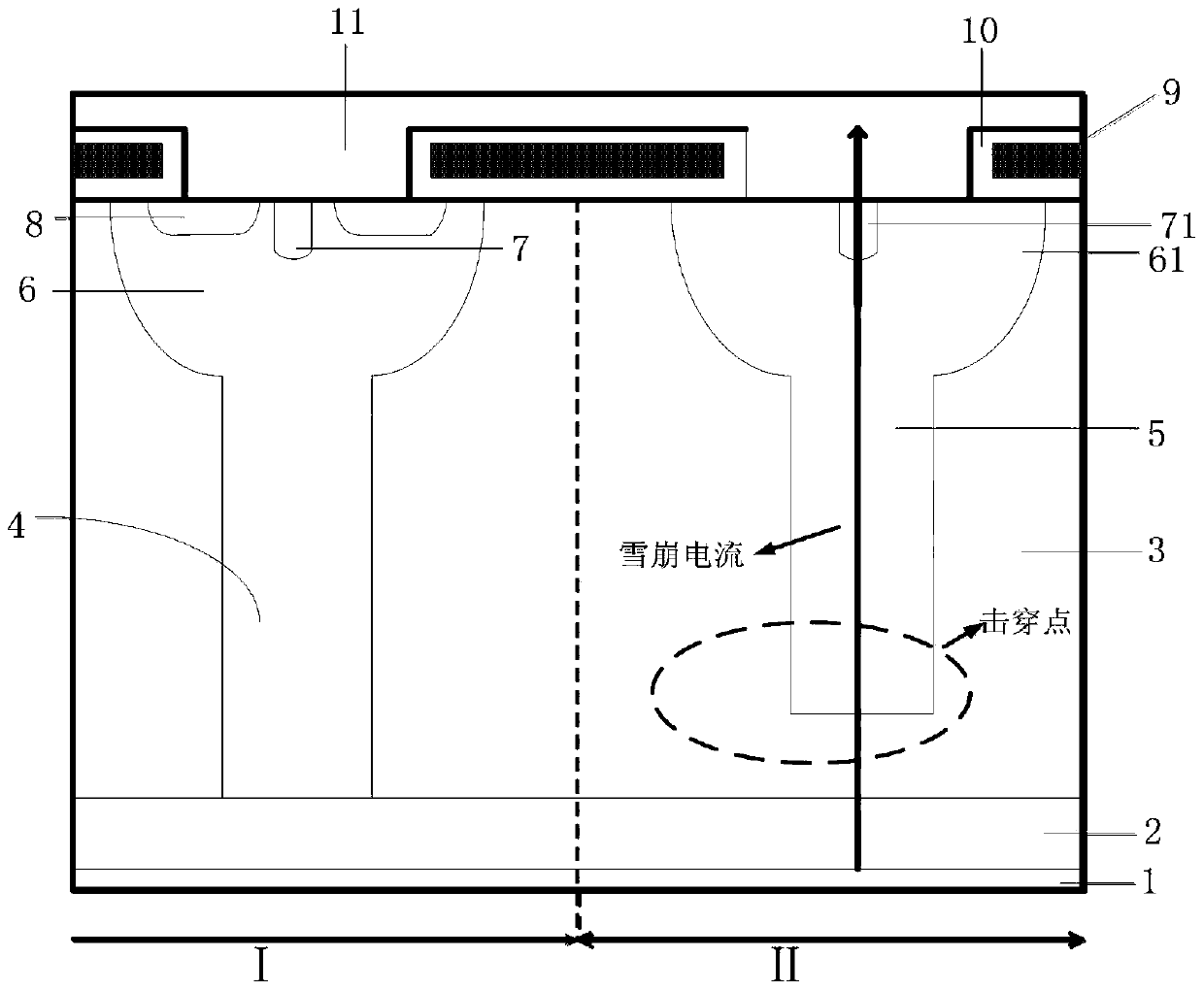
[0028] Such as image 3As shown, this example includes normal cell area I (only one cell is shown in the figure) and pseudo cell II; the normal cell area I and pseudo cell II share the same metal drain electrode 1, metal drain electrode 1 Above is the N+ substrate 2, and above the N+ substrate 2 is the N epitaxial region 3; the N epitaxial region 3 has the first P-type column 4 in the normal cell and the second P-type column 5 in the dummy cell ; The first P-type column 4 and the N epitaxial layer 3 of the normal cell meet the charge balance, the top of the first P-type column 4 is the first P-type body region 6, and the N+ active region 8 is located inside the first P-type body region 6 And connected to the source electrode 11, there is a P+ contact region 7 also connected to the source electrode 11 between the N+ active regions 8; the second P-type column 5 of the pseudo-cell is the same as the doping concentration of the first P-type column 4 and the second P-type column 4 ...

Embodiment 3

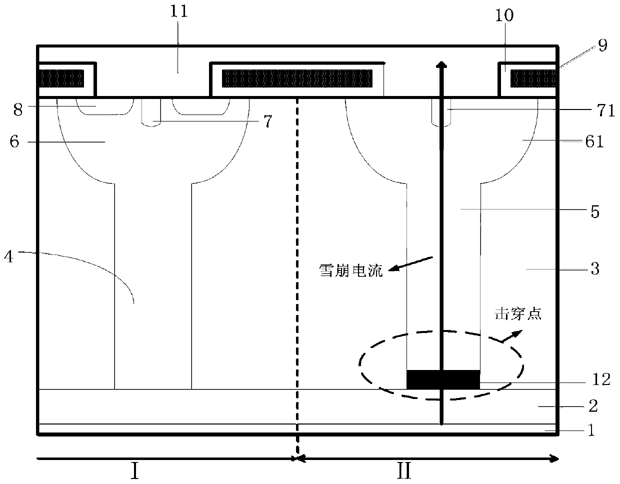
[0030] Such as Figure 4 As shown, this example includes normal cell area I (only one cell is shown in the figure) and pseudo cell II; the normal cell area I and pseudo cell II share the same metal drain electrode 1, metal drain electrode 1 Above the N+ substrate 2, on the N+ substrate 2 is the N epitaxial region 3; the N epitaxial region 3 includes the first P-type column 4 in the normal cell and the second P-type column 5 in the dummy cell ; The first P-type column 4 and the N epitaxial layer 3 of the normal cell meet the charge balance, the top of the first P-type column 4 is the first P-type body region 6, and the N+ active region 8 is located inside the first P-type body region 6 And connected to the source electrode 11, there is a P+ contact region 7 also connected to the source electrode 11 between the N+ active regions 8; the second P-type column 5 of the pseudo-cell is the same depth as the first P-type column 4 and the second P The overall concentration of the pilla...


PUM


Abstract

The invention relates to power semiconductor technology, in particular to a super junction MOSFET. The difference between the present invention and the conventional super junction MOSFET is that a pseudo cell composed of a second P-type column (5) is arranged next to one or more conventional super junction cells, the pseudo cell does not contain an N+ active region, And the length of the P column is appropriately shortened compared with the normal cell; or the length of the P column is the same as that of the normal cell, but there is a region with a relatively high doping concentration at the bottom near the substrate; or the overall doping concentration of the P column is slightly higher than that of the normal cell. P-pillars of other cells. When an avalanche breakdown occurs, the breakdown voltage of the dummy cell will be slightly lower than that of the normal cell, the avalanche breakdown point will be limited to the dummy cell, and the avalanche current will flow out through the source electrode of the dummy cell. Since the pseudo-cell does not contain an N+ active region and there is no parasitic BJT, the conduction of the parasitic BJT is avoided, so the avalanche tolerance and reliability of the super-junction MOSFET device can be improved.

Description

technical field [0001] The invention relates to power semiconductor technology, in particular to a super junction MOSFET. Background technique [0002] Power MOSFET (Metal Oxide Semiconductor Field Effect Transistor) plays an important role in various power conversions, especially in high-frequency power conversions, due to its advantages of high switching speed, low switching loss, and low driving loss. The switching process under an unclamped inductive load (Unclamped Inductive Switching, UIS) is generally considered to be the most extreme electrical stress situation that power devices can encounter in system applications. Because the energy stored in the inductor must be released by the power device at the moment of turn-off when the loop is turned on, and the high voltage and high current applied to the power device can easily cause the device to fail. Avalanche endurance is an important parameter to measure the ability of a device to resist UIS. [0003] There are two...

Claims


Application Information

Patent Timeline
Patent Type & Authority Patents(China)
IPC IPC(8): H01L29/06H01L29/78
CPCH01L29/0634H01L29/7827
Inventor 任敏王亚天陈哲曹晓峰李爽李泽宏张金平高巍张波
Owner UNIV OF ELECTRONICS SCI & TECH OF CHINA
Why Eureka
Try Eureka