Preparation method of trench grid VDMOS (vertical double-diffused metal oxide semiconductor) device with ultra-thin source region

A source area and device technology, applied in semiconductor/solid-state device manufacturing, electrical components, circuits, etc., can solve problems such as limitations and difficulties, and achieve the effects of saving manufacturing costs, reducing parasitic resistance, and improving the ability to resist UIS failures

Inactive Publication Date: 2014-12-03
UNIV OF ELECTRONICS SCI & TECH OF CHINA +1
View PDF6 Cites 0 Cited by
  • Summary
  • Abstract
  • Description
  • Claims
  • Application Information

AI Technical Summary

Problems solved by technology

but reduce N + The width of the source region is limited by the lithography precision, and there are certain difficulties

Method used


Image

  • Preparation method of trench grid VDMOS (vertical double-diffused metal oxide semiconductor) device with ultra-thin source region
  • Preparation method of trench grid VDMOS (vertical double-diffused metal oxide semiconductor) device with ultra-thin source region
  • Preparation method of trench grid VDMOS (vertical double-diffused metal oxide semiconductor) device with ultra-thin source region

Examples


Embodiment Construction

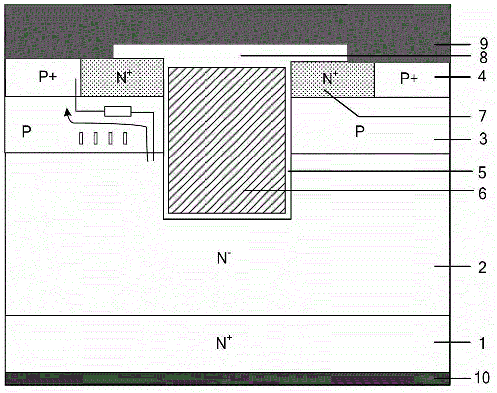
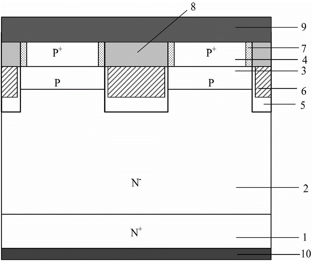
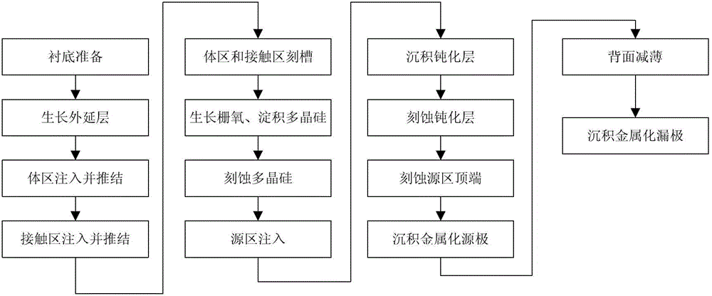
[0038] The process steps of a specific embodiment of a trench gate type VDMOS with an ultra-thin source region are described in detail below:

[0039] 1. Preparation of single crystal silicon, using N-type heavily doped single crystal silicon substrate 1, the doping concentration is 1.6×10 19 cm -3 , and its crystal orientation is .

[0040] 2. To grow the epitaxial layer, use the vapor phase epitaxy VPE method to grow 15μm N on the substrate 1 at a temperature of 1000 ℃ and a vacuum condition - Epitaxial layer 2, phosphorus doping concentration is 3.5 × 10 15 cm -3 .

[0041] 3. Boron ion implantation and push junction, using high-energy boron ion implantation with energy of 120KeV and a dose of 1×10 13 cm -2 , form P-type body region 3, and perform high-temperature push junction, so that the junction depth of P-type body region 3 is about 1.2 μm; use boron ion implantation with an energy of 100KeV and a dose of 2 × 10 15 cm -2 , forming P + Contact area 4, P + The ...


PUM


Abstract

The invention discloses a preparation method of a trench grid VDMOS (vertical double-diffused metal oxide semiconductor) device with an ultra-thin source region, belonging to the manufacturing field of semiconductor devices and processes. By using an inclined angle ion implantation technique, the VDMOS device with the ultra-thin source region can be obtained by only utilizing two photoetching masks, so that the manufacturing cost is saved; and the formation of the ultra-thin source region is not limited by the photoetching precision, in other words, the ultra-thin source region can be made extremely narrow, so that the opening of a parasitic BJT (bipolar junction transistor) in the trench grid VDMOS device is prevented effectively, and the UIS (unclamped inductive switching) failure-resistant ability of the device is improved.

Description

technical field [0001] The invention belongs to the technical field of semiconductor device and process manufacturing, and relates to a preparation method of a trench gate type VDMOS device. Background technique [0002] At present, the application fields of power semiconductor devices are becoming wider and wider, and can be widely used in DC-DC converters, DC-AC converters, relays, motor drives and other fields. Compared with bipolar transistors, vertical double-diffused metal-oxide-semiconductor field-effect transistors (VDMOS) have the advantages of fast switching speed, low loss, high input impedance, low driving power, good frequency characteristics, and highly linear transconductance. In particular, VDMOS has a negative temperature coefficient, there is no secondary breakdown problem of bipolar transistors, and the safe working area is large, so its application range is wider. [0003] In the design of automotive electronics, switching power supplies and DC-DC conver...

Claims


Application Information

Patent Timeline
Patent Type & Authority Patents(China)
IPC IPC(8): H01L21/336
Inventor 任敏张灵霞邓光敏张蒙赵起越李泽宏张金平张波
Owner UNIV OF ELECTRONICS SCI & TECH OF CHINA
Why Eureka
Try Eureka