Imaging method, imaging device and electronic device

An imaging device and imaging method technology, which are applied in the fields of image sensors, imaging methods, imaging devices and electronic devices, can solve problems such as affecting imaging effects, poor photographing effects, and failing to capture scenes, and improve clarity and signal-to-noise ratio. , Brightness and clarity, complete color and vivid effect

Active Publication Date: 2017-06-13
GUANGDONG OPPO MOBILE TELECOMM CORP LTD
View PDF4 Cites 0 Cited by
  • Summary
  • Abstract
  • Description
  • Claims
  • Application Information

AI Technical Summary

Problems solved by technology

[0002] Existing RGB image sensors have poor, blurry, or even blurry pictures in low-light conditions
Some image sensors are embedded with infrared filter pixels to provide imaging effects, but when the light is sufficient, infrared rays entering the image sensor will affect the imaging effect, causing color casts in the image, etc.

Method used


Image

  • Imaging method, imaging device and electronic device
  • Imaging method, imaging device and electronic device
  • Imaging method, imaging device and electronic device

Examples


Embodiment Construction

[0049] Embodiments of embodiments of the present invention are described in detail below, examples of which are shown in the drawings, wherein the same or similar reference numerals designate the same or similar elements or elements having the same or similar functions throughout. The embodiments described below by referring to the drawings are exemplary, are only for explaining the embodiments of the present invention, and should not be construed as limiting the embodiments of the present invention.

[0050] The imaging method, image sensor, imaging device and electronic device according to the embodiments of the present invention will be further described below with reference to the accompanying drawings.

[0051] see figure 1 , the imaging method of the embodiment of the present invention comprises the following steps:

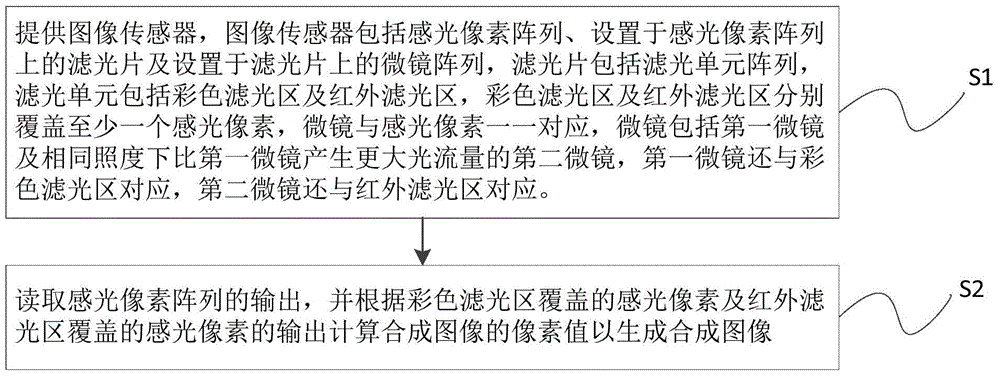
[0052] S1, providing an image sensor, the image sensor includes a photosensitive pixel array, a filter arranged on the photosensitive pixel array, and a m...


PUM


Abstract

The invention discloses an imaging method. First, an image sensor is provided. The image sensor includes a photosensitive pixel array, a light filter arranged on the photosensitive pixel array, and a micromirror array arranged on the light filter. The light filter includes a light filter The unit array, each filter unit includes a color filter area and an infrared filter area. The micromirrors are in one-to-one correspondence with the photosensitive pixels. The micromirrors include a first micromirror and a second micromirror that produces a greater light flux than the first micromirror under the same illumination. The first micromirror and the second micromirror are respectively connected to the color filter area corresponds to the infrared filter area. Next, the output of the photosensitive pixel array is read, and the pixel values ​​of the composite image are calculated according to the outputs of the photosensitive pixels covered by the color filter area and the photosensitive pixels covered by the infrared filter area to generate a composite image. The resulting composite image contains complete color information and has a high signal-to-noise ratio. The invention also discloses an image sensor, an imaging device and an electronic device which can be used to realize the imaging method.

Description

technical field [0001] The invention relates to imaging technology, in particular to an imaging method, an image sensor, an imaging device and an electronic device. Background technique [0002] Existing RGB image sensors have poor photo effects, blurry, or even blurry pictures under low illumination. Some image sensors are embedded with infrared filter pixels to provide imaging effects, but when the light is sufficient, infrared rays entering the image sensor will affect the imaging effect, causing color casts in the image, etc. Contents of the invention [0003] The present invention aims to solve at least one of the technical problems existing in the prior art. Therefore, the present invention needs to provide an imaging method, an image sensor, an imaging device and an electronic device. [0004] The imaging method of the embodiment of the present invention comprises the following steps: [0005] An image sensor is provided, the image sensor includes an array of pho...

Claims


Application Information

Patent Timeline
Patent Type & Authority Patents(China)
IPC IPC(8): H04N9/07H04N5/225H04N5/359
CPCH04N23/57H04N25/62H04N23/12
Inventor 范宇
Owner GUANGDONG OPPO MOBILE TELECOMM CORP LTD
Why Eureka
Try Eureka