Semiconductor structure and forming method thereof

A technology of semiconductor and isolation structure, applied in the field of semiconductor structure and its formation, can solve the problems of device failure, difficult to stabilize control, complex manufacturing process, etc., and achieve the effect of avoiding failure and high resistance

Active Publication Date: 2016-06-08
SEMICON MFG INT (SHANGHAI) CORP
View PDF4 Cites 2 Cited by
  • Summary
  • Abstract
  • Description
  • Claims
  • Application Information

AI Technical Summary

Problems solved by technology

[0004] Although the introduction of gate dielectric layers and metal gates including high-k materials and metal materials can improve the electrical performance of semiconductor devices, it has been found in practical applications that due to the continuous shrinking of the device geometry, the manufacturing process is complicated and difficult to control stably. prone to device failure

Method used


Image

  • Semiconductor structure and forming method thereof
  • Semiconductor structure and forming method thereof
  • Semiconductor structure and forming method thereof

Examples


Embodiment Construction

[0036] It can be seen from the background art that in the prior art, in the manufacture of semiconductor devices with metal gates, the manufacturing process is complicated and difficult to control stably, which easily leads to device failure.

[0037] For further illustration, the present invention provides an embodiment of a semiconductor structure.

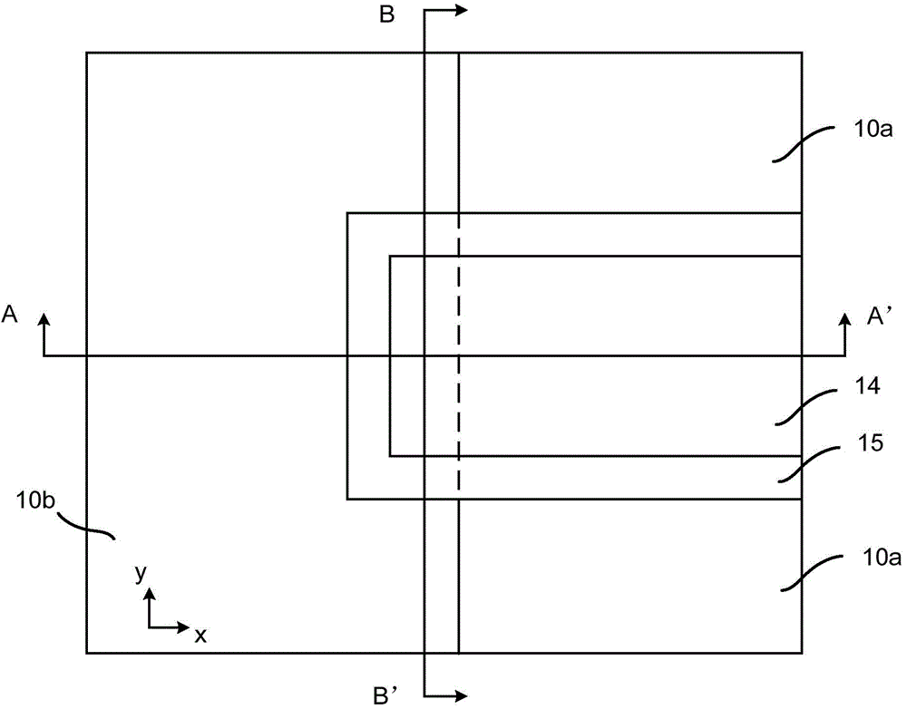
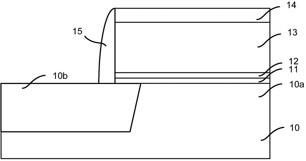
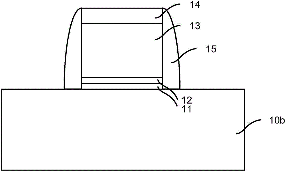
[0038] Please refer to figure 1 , figure 2 and image 3, provide a semiconductor substrate 10, the surface of the semiconductor substrate 10 is formed with a gate structure and sidewalls 15 located on the side walls of the gate structure, the gate structure includes a gate dielectric layer located on the surface of the semiconductor substrate 10, A gate layer 13 located on the surface of the gate dielectric layer and a mask layer 14 located on the surface of the gate layer 13 . in, figure 1 is a top view of the semiconductor structure, figure 2 for figure 1 Schematic diagram of the cross-sectional structure along the ...


PUM


Abstract

The invention provides a semiconductor structure and a forming method thereof. The forming method of the semiconductor structure comprises the following steps: a semiconductor substrate comprising an active region structure and a shallow trench isolation structure is provided; a gate structure and spacers on the sidewalls of the gate structure are formed on the surface of the semiconductor substrate, the gate structure comprises a gate dielectric layer on the surface of the semiconductor substrate, the gate dielectric layer comprises a dielectric layer on the surface of the semiconductor substrate and a metal layer on the surface of the dielectric layer, and part of the gate structure and part of the spacers are disposed on the surface of the shallow trench isolation structure; and part of the metal layer on the shallow trench isolation structure is modified to make the part of the metal layer converted into a protective layer. The protective layer protects the gate dielectric layer on the surface of the active region structure from being corroded and consumed by acid, and failure of semiconductor devices is avoided.

Description

technical field [0001] The invention relates to the field of semiconductor manufacturing, in particular to a semiconductor structure and a forming method thereof. Background technique [0002] With the rapid development of integrated circuit manufacturing technology, the technology nodes of semiconductor devices are constantly decreasing, and the geometric dimensions of devices are also shrinking continuously following Moore's Law. When the size of the semiconductor device is reduced to a certain extent, various problems caused by the semiconductor device approaching the physical limit appear one after another. In the field of semiconductor device manufacturing, the most challenging problem is how to solve the problem of device reliability degradation, which is mainly caused by the continuous reduction of the thickness of the traditional gate dielectric layer. The method provided by the prior art replaces traditional gate dielectric materials with high-k gate dielectric mat...

Claims


Application Information

Patent Timeline
Patent Type & Authority Applications(China)
IPC IPC(8): H01L21/336H01L29/78
Inventor 何永根
Owner SEMICON MFG INT (SHANGHAI) CORP
Why Eureka
Try Eureka